Historically, the interest in GaN based semiconductor devices was sparked by the development of blue LEDs by Akasaki, Amamano, and Nakamura [29]. Soon after the discovery of the formation of a native 2DEG in UID
GaN/AlGaN heterostructures [30], already the first HFET was built [31]. Because of the large sheet carrier density of about  1/cm2 and the high electron mobilities in the channel, this kind of devices are usually also called HEMT.
Up to date, the majority of the HEMTs are built on Ga-face GaN and show normally-on behavior, meaning that a negative voltage has to be applied in order to turn them off. However, due to safety reasons in case of driver failures, normally-off devices are the preferred choice for power applications. Since the 2DEG is formed natively, the design of normally-off devices with comparably high performance is still an essential task for research groups around the world.
This section briefly addresses the physics behind the formation of the 2DEG due to the polarization charges as well as the compensation mechanism of the electrons in the channel. Afterwards, the design principles of current normally-on and normally-off HEMTs are discussed in Sections 2.3.2 and 2.3.3.
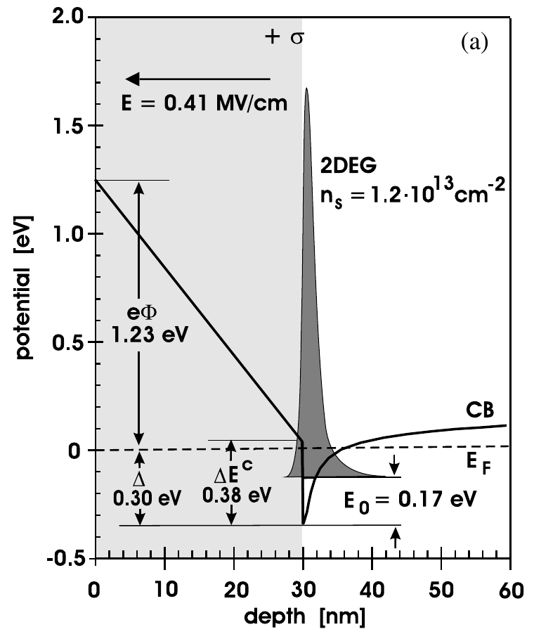
The formation of an intrinsic 2DEG at a high-quality GaN/AlGaN interface with improved carrier mobilities was first discovered by Khan in 1991 [30]. During the following years, the source of the electrons forming this electron channel was a matter of intense debate. To understand the confusion about the source of the electrons, it is advisable to come back to the polarization induced charges presented above. In Figure 2.5 a complete heterostructure including the induced sheet carrier densities is shown together with a self-consistent solution of the conduction band edges from [27].

 Ga
Ga heterostructure with the sign and position of polarization induced sheet carrier densities. The red arrows stand for positive and the blue ones for negative sheet charges. Right: Self-consistent solution of the structure on the left with the polarization charges and the Schottky barrier of nickel for
layer thicknesses of 2000 nm and 30 nm, respectively (from [27]).
heterostructure with the sign and position of polarization induced sheet carrier densities. The red arrows stand for positive and the blue ones for negative sheet charges. Right: Self-consistent solution of the structure on the left with the polarization charges and the Schottky barrier of nickel for
layer thicknesses of 2000 nm and 30 nm, respectively (from [27]).
The source of the free electrons cannot be found in polarization charges, as their net charge across the whole device is zero. In addition, the energy per unit area in a polarized material with the thickness  is given by [6]
According to this equation, the energy stored in the crystal structure scales linearly during growth. Due to energy minimization, the polarization charges will be neutralized if the energy exceeds the bandgap of the material. This value is usually called the critical thickness of polarized materials. It can be seen as an upper limit beyond which the polarization charges are going to be neutralized by some kind of defects during growth. For free-standing GaN, this critical thickness is about 10 nm, clearly favoring a local compensation of the polarization induced sheet charges at the surface region between the substrate and GaN. The same argument holds for the AlGaN layer, usually also referred to as the barrier region, as the local energy minimization at the AlGaN surface can be fulfilled either by adsorbates for freestanding surfaces or the next metal or passivation layers for fully processed devices.
Up to date, the most widely accepted model to explain the source of the electron channel is the surface donor model, proposed by Ibbetson in 2000 [32]. It follows a chain of simple charge neutrality arguments which can be outlined as follows:
• In the absence of an external electric field, the sum of all space charges present in any as-grown device needs to be zero. Since the polarization induced sheet charges form a dipole, their sum also has to be zero.
• According to the critical thickness argument discussed before, the positive polarization charges at the substrate are compensated locally. The fact that the electrons are confined in a 2DEG without external fields rules out the same mechanism for the GaN/AlGaN interface.
• If the electrons were primarily generated thermally in the GaN buffer due to unintentional doping or point defects, the 2DEG would also not be confined.
• The confinement of electrons in the 2DEG is, however, experimentally well proven by CV profiles [33].
• Thus, the only two charge contributions left to compensate for the channel electrons are bulk defects in the barrier layer and surface defects. The dominant part of these two contributions can only be the surface states. For typical barrier thicknesses of 10 nm to 20 nm, the effective barrier doping
would need to be on the order of  1/cm3, which would significantly degrade the channel mobility.
• The dominantly donor-like behavior of the defects stems from the fact that their net charge needs to be positive when ionized in order to compensate for the electrons.
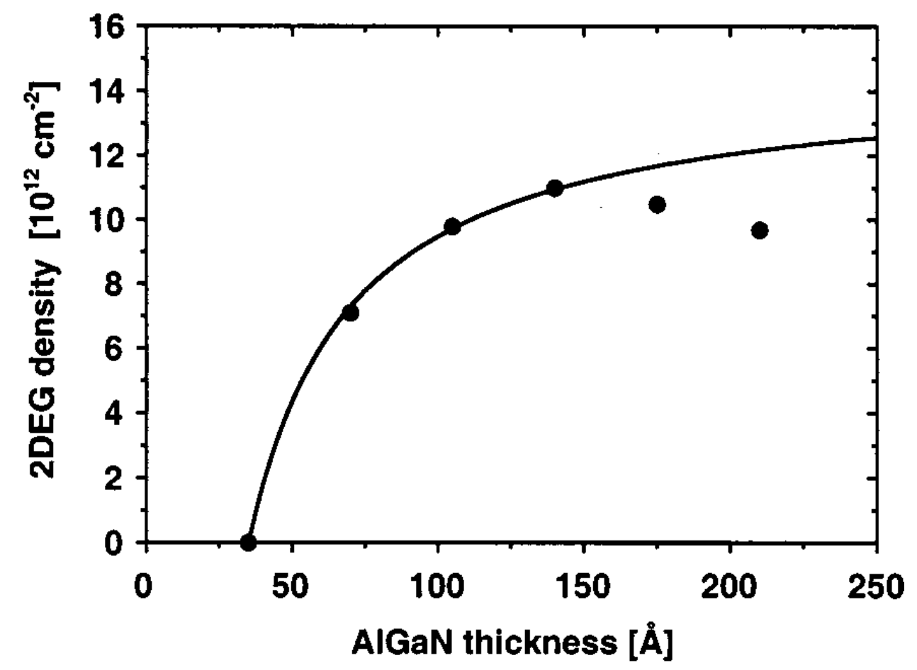
• The polarization induced barrier field introduces a dependence of the surface potential on the barrier thickness. Thus the position of a pre-existing defect distribution is a function of the barrier thickness. That means if the barrier is below a certain critical thickness, all donors are below the Fermi level and no 2DEG is going to be formed (see also Figure 2.6).
• Conversely, the defects could also be formed during growth above a certain threshold due to energy minimization following (2.25) and the following discussion. The consequences for the induced electron channel would essentially be the same as for pre-existing defects.


 Ga
Ga heterostructure. The deviation from the theoretical values can most likely be explained by partial strain relaxation for thicker AlGaN barriers (from [32]).
Despite being the widely accepted model for the formation of the 2DEG, the surface donor model is a purely phenomenological model. It provides no information about the structure, distribution and dynamic behavior of the defects. If ionized donors in the barrier layer are neglected, the surface donor model gives a lower bound to the defect density at the interface, which must then correspond to the sheet carrier density in the channel.
The first GaN/AlGaN HEMT was built using a 100 nm thick barrier layer with 14 % Al content on top of a 600 nm thick GaN layer grown on sapphire [31]. The ohmic contacts in HEMTs are manufactured to have direct contact to the 2DEG with no need for additional doping implants. The native 2DEG thus is used as the transistor channel. The gate was initially placed directly on the AlGaN layer forming a Schottky contact. A device schematic of such a device is shown in Figure 2.7 (left).
During the following years, devices with ever-increasing microwave performance were demonstrated [34, 35]. All of these devices were suffering from severe current dispersion effects (i.e. the temporal reduction of the on-current) due to charge trapping in the buffer and at the AlGaN surface. The first strategy to address this problem was to minimize dislocation density in the buffer by optimizing the substrate nucleation layers. Further progress in the suppressing the dispersion was achieved by depositing SiN passivation layers on the surface of the devices [36–38] and using field plates to reduce the electric fields at the drain side of the gate during high voltage operation [39, 40].
There are, however, downsides in using Schottky contacts for the transistor gate. The most prominent one is the increased gate leakage currents especially in the off-state at high reverse gate biases [41, 42]. Another problem in switching applications is called back EMF coming from the load, which potentially can reverse the gate diode for a short timespan and damage the device. An insulating layer placed between the barrier and the gate contact addresses these problems. Such devices are usually called MIS-HEMT and were first demonstrated by Khan in 2003 [43]. A schematic representation of a GaN MIS-HEMT can be seen in Figure 2.7 (right).
The additional AlGaN/dielectric interface underneath the gate nevertheless introduces an additional problem: Due to the Fermi level pinning of the gate in Schottky devices, the effect of surface donors is mostly limited to the access regions of the device causing current dispersion. Because of the insulator underneath
the gate, these defects now become relevant in terms of  shift, especially under forward bias conditions [6, 44].
Normally-off devices are the preferred choice in power switching applications because of safety reasons in the case of driver failures. Since regular GaN HEMTs naturally show normally-on behavior, special concepts are needed to fabricate enhancement mode transistors. This section briefly introduces the three most common concepts together with their individual benefits and drawbacks.
One of the first approaches to create normally-off devices was to perform a recess etch of the barrier layer before the deposition of the gate [45, 46]. For the first demonstrated devices, the barrier layer underneath the gate was removed completely, leaving behind a regular GaN FET based on the unintentional doping of the buffer layer. If a Schottky gate is used directly on this channel, the achievable threshold voltage is smaller than 1 V with limited gate swing due to turn on of the gate diode.
These problems can be mitigated by the formation of a regular MOSFET structure, see Figure 2.8. The main drawback of fully recessed devices is that the barrier layer needs to be sacrificed to obtain normally-off operation. Such devices thus cannot utilize one of the main benefits of the GaN/AlGaN structures, which is the high-density, high-mobility 2DEG at the heterointerface. Consequently, these devices often suffered from poor performance regarding the channel resistance. The design of devices with shorter channel lengths to lower the channel resistance only solved parts of the problems as trade-offs against the breakdown voltage needed to be made. More recent concepts use hybrid approaches between a partly recessed barrier layer and an additional fluorine implantation step [47, 48].

Another concept to realize enhancement mode HEMTs is to treat regular depletion mode devices with an additional fluorine implant prior to the formation of the gate, see Figure 2.9 and [49–51], or partly recess etched devices together with implantation to enlarge and enhance reliability [47, 48].
To be effective, the implantation has to incorporate the fluorine atoms into the barrier layer. Fluorine mostly stabilizes in interstitial positions in the crystal where it tends to capture a free electron due to its large electronegativity. Thus it can be seen as a fixed negative charge which compensates parts of the positive polarization charges and therefore depletes the 2DEG underneath the gate.
The main benefit of this method is that comparably large values of up to 4 V can be achieved. Because it only consists of one additional processing step, normally-off devices can be created using the same device schemes as regular HEMTs or MIS-HEMTs. Unlike other methods, the high-quality 2DEG is mostly preserved although the scattering of channel
electrons can potentially be increased due to the fluorine charges. A judgment about the amount of fluorine induced scattering is tricky, since normally-on and normally-off devices from the same technology need to be compared. In [50], a  degradation of about 10 % was reported while the devices in [49] showed no degradation at all after annealing.

shift can be reliably controlled by the implantation time.
Another concept to obtain enhancement mode devices is called gate injection transistors, which are shown in Figure 2.10. They use a p-doped GaN layer underneath the gate to deplete the 2DEG in this region, allowing to obtain normally-off operation with threshold voltages of about 1 V to 2 V. The devices typically possess two regions of operation, one being similar to a conventional JFET for low voltages and an additional increase of conductivity at higher voltages caused by hole injection into the GaN/AlGaN interface from the p-GaN layer [52, 53].
Because of charge neutrality, every hole injected into the channel produces an equal amount of electrons in the 2DEG. Due to the larger electron mobility, the holes tend to remain around the gate while the electrons contribute to the drain current. Since the AlGaN barrier blocks electron injection into the gate, these devices allow low gate leakage currents while maintaining high drain currents.


