In this chapter, the essential models which will be used to describe BTI phenomena throughout this work are presented. After a brief explanation of CET maps being a clever way to visualize experimental eMSM data in Section 5.1, the theoretical foundation of the NMP theory to describe charge trapping is discussed in Section 5.2.1. Some evidence for the importance of phonon-assisted charge transitions in oxide defects and the framework of the well-known NMP four-state model and the derivation of equations for the time-constants is covered in Section 5.2.2. Section 5.2.3 introduces an extension to the NMP theory for charge trapping in semiconductors by also including the interactions with the local bands.
When performing eMSM measurements, the recorded stress and recovery traces contain detailed information about the active defects at a given temperature and bias condition [100]. One way to visualize the capture and emission times of the
active defects and their impact on  is using CET maps [115, 118, 119]. In the case of large-area devices,
the response of the individual active defects per area
is using CET maps [115, 118, 119]. In the case of large-area devices,
the response of the individual active defects per area  is grouped together into a density
  defined as [110]
with  being the individual step height,
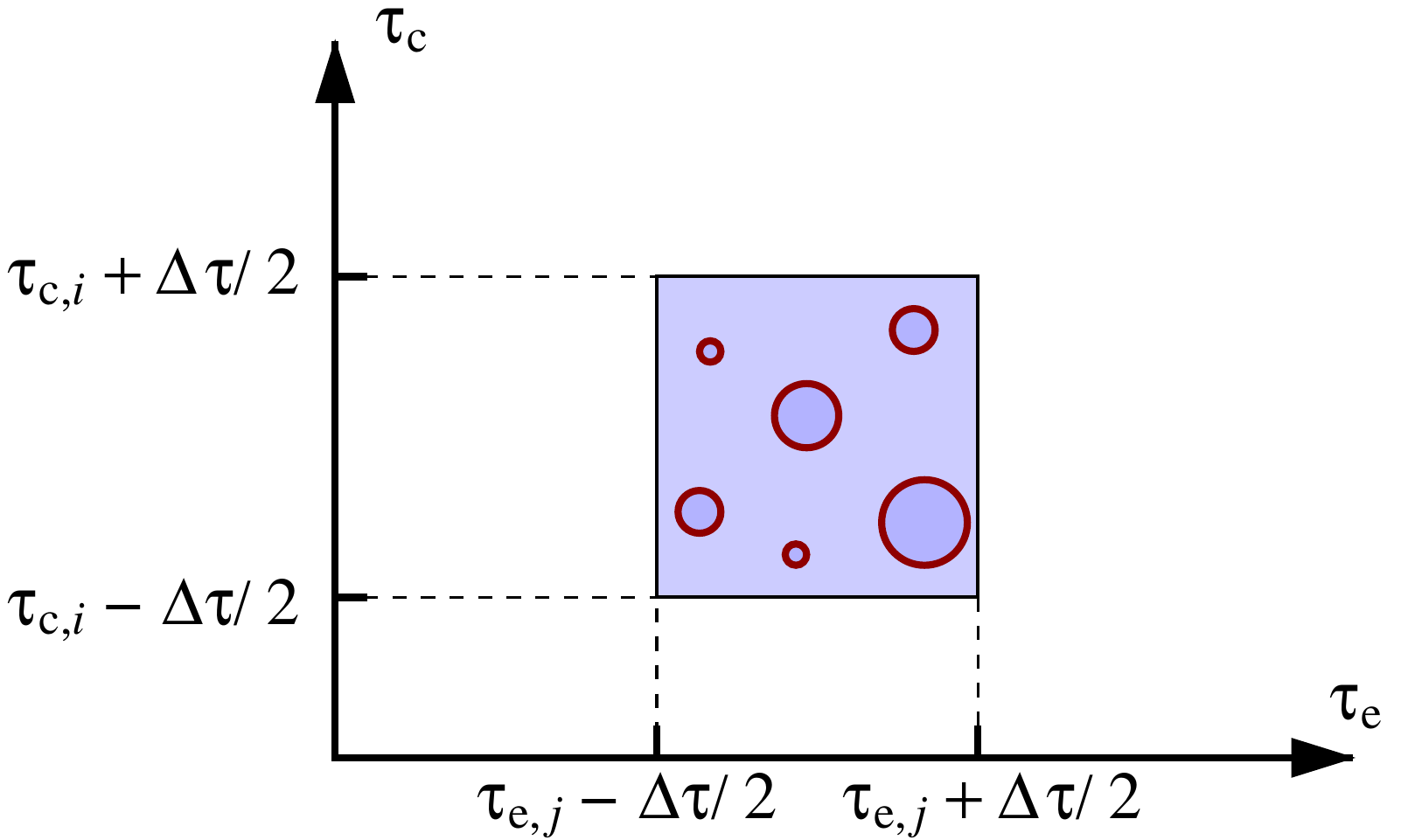
  the maximum occupancy change of the defect and the rectangle functions
With this definition, (5.1) simply collects all defects within a certain area of  and
and  into (see Figure 5.1). The change in the occupancy after stressing for
  seconds and
  seconds of recovery, normalized by the maximum change in occupancy is given by [110]
The total degradation can be calculated by summing over all capture and emission times.
In the limit  , the rectangle functions in (5.1) can be replaced by Dirac functions. If the exponential terms in (5.3) are replaced by two unit step functions around and , one obtains a simple relationship between between
  and
and  [110]:
In other words, the degradation is obtained by summing up all the defects being charged until , but not yet discharged after . This means that the can easily be obtained directly from the measurements by calculating the mixed partial derivative of the measured stress and recovery traces [110] as
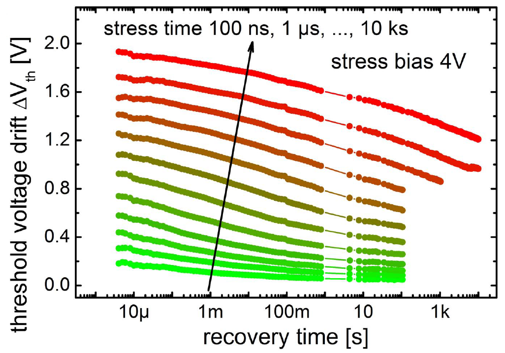
Thus, the density in the CET maps stands for the capture and emission times of the defects weighted by their individual impact on . It should be noted that the data in a CET map in general is only valid for a particular set of stress and recovery biases at a specific temperature. In large-area devices where a lot of defects contribute to , CET maps are usually used to visualize the average response of a large number of defects for a certain technology at a certain stress condition. An example for a CET map obtained from eMSM measurements on GaN MIS-HEMTs is given in Figure 5.2.