The long-term stability of GaN/AlGaN HEMTs today is still the main problem prohibits a wider market adoption. Many of the observed degradation phenomena are related to charge trapping and thus especially detrimental to the dynamic response of the devices [67–69]. As in every technology, the different degradation mechanisms overlap during regular operation. To identify the responsible mechanism and extract certain defect parameters, special attention has to be paid to the extraction methodology as well-established characterization schemes for silicon often fail for GaN devices.
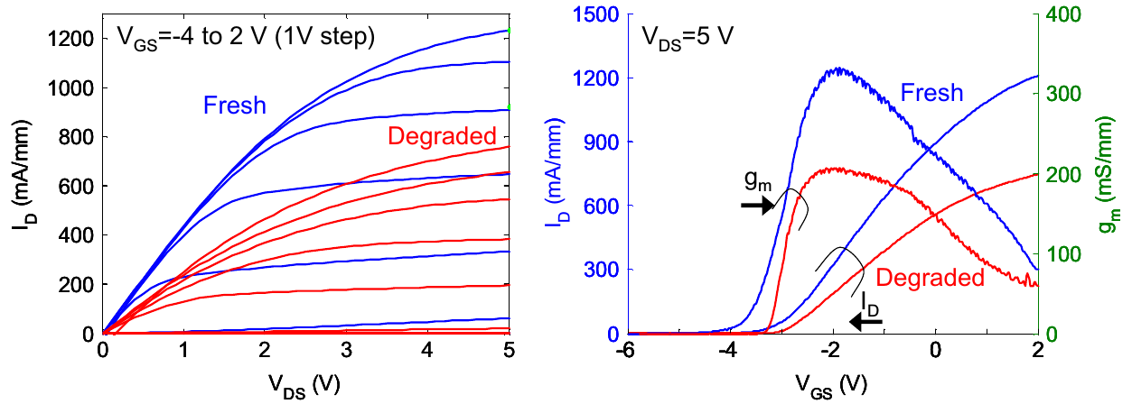
One of the first degradation mechanisms investigated in GaN devices was the transient drain current dispersion after applying a voltage step to the gate or the drain [67, 70]. An example of the observed degradation can be seen in Figure 3.3. To study the nature and the location of the defects responsible for this type of degradation, the drain current is monitored using single or double pulsed drain current measurements to obtain the transient response after a certain stress condition was applied [71, 72]. This method is often also referred to as drain current transient spectroscopy.
Current collapse is usually investigated at different temperatures with the devices being in the off-state and with high biases applied to the drain. Under these bias conditions, bulk and surface defects residing at the drain sided access regions can be investigated [68, 69, 73]. By changing the bias conditions, defects residing in different areas of the device can
be explored. If, for example, all terminals are grounded and a negative substrate bias is applied, defects in the whole buffer region contribute and a mixture between  drift and current collapse will be observed [68]. The degradation can be evaluated equivalently either in terms of transient drain current,
  or
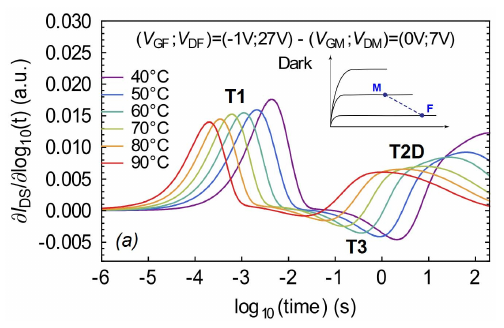
or  behavior. From this data, defect properties like the apparent activation energy and capture cross-sections can be extracted. A proper selection of temperature, bias conditions and filling pulses thus allows conducting a full defect spectroscopy [73]. An example of the cross-sections and apparent activation energies of three bulk defect levels extracted by this method is given in Figure 3.4.
Threshold voltage drift can in general be caused by all kinds of defects residing underneath the gate. A negative shift can be caused for example by positively charged defects in the GaN buffer when applying negative biases at the gate or the substrate. This mechanism is usually attributed to a local modulation of the buffer potential by acceptor defects used for buffer compensation [68, 73]. Other works attribute NBTI in MIS-HEMTs mainly to electron emission from the partially charged surface donors at the gate [74]. Because of the absence of the electron channel shielding the buffer defects from the defects at the barrier and the interface, the dominant of the two mechanisms can only be determined by the extracted defect properties.
On the other hand, PBTI in normally-on devices is only observed for positive gate bias conditions, ruling out the influence of buffer traps because of the strong shielding due to the electron channel [65, 74, 75]. It was shown that the amount of charge being captured at the dielectric interface under PBTI stress is only limited by the theoretical value calculated from
the dielectric capacitance rather than by the interface defect density [66]. When assuming that all charges are stored at the dielectric interface, the maximum amount of charge which can be stored in the dielectric capacitor  per unit area is
  . The amount of trapped charges at that interface
  is
is
Figure 3.5 shows that the amount of drift and thus the trapped charges almost reaches the theoretical limit for many devices with different dielectric materials and heights. This suggests that the density of accessible interface states is always higher than the amount of charges stored at the dielectric interface, which is consistent with the
predictions coming from the surface donor model discussed in Section 2.3.1.

. This suggests that the interface trap density is higher than  for all of the investigated cases (from [66]).
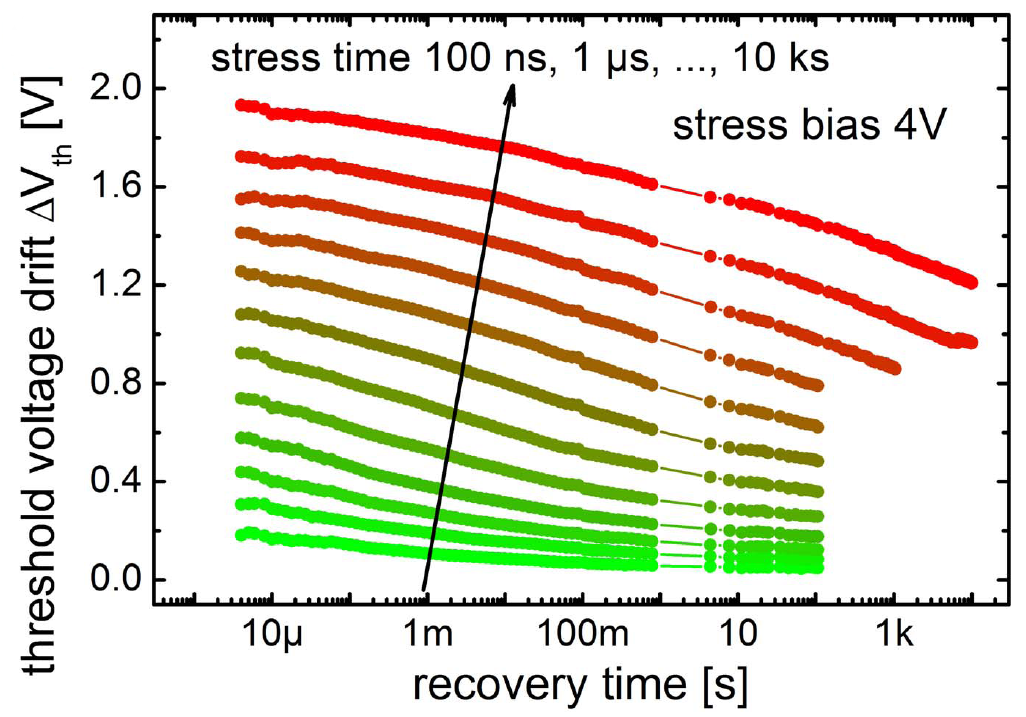
Studies on the stress and recovery dynamics of interface defects in GaN MIS-HEMTs show that there is almost a logarithmic relationship of the PBTI drift over time for both, stress and recovery [65, 74, 75]. This indicates a very broad distribution of capture and emission time constants of the surface defects as shown in Figure 3.6. There is still a fair amount of uncertainty on whether the observed time constants stem from intrinsic defect properties or if other effects like the transport through the barrier or charge feedback effects obfuscate the extraction of the real capture and emission times [AGJ1, AGC1][65, 74]. A thorough investigation of charge feedback effects on the recovery kinetics of PBTI in GaN will be presented in Section 7.1.3 of this work.

Recent publications have revealed another type of degradation of GaN HEMTs which is most prominent in semi-on conditions (i.e. weak channel together with high drain voltages). These conditions are typically considered the worst-case conditions for hot carrier related phenomena throughout the literature.
Measurements of the degradation in off-state conditions compared to semi-on conditions revealed an additional charge trapping mechanism which is usually attributed to bulk defects in the buffer or the barrier (see Figure 3.7). The proposed mechanism is that hot electrons are able to escape from the confinement in the channel and subsequently get captured in pre-existing bulk defects [68, 76, 77]. A recent study delivers solid experimental evidence for channel hot electrons and
impact ionization present in N-face GaN HEMTs using electroluminescence in conjunction with the gate currents [78]. Unfortunately this study does not deliver any other information on the observed device degradation except of the elevated
gate currents.
As opposed to silicon technology [AGC2, AGJ2], experimental studies on long-term damage caused by channel hot carriers are still missing for GaN technology. One degradation mechanism potentially creating permanent damage at high fields was proposed by del Alamo [67]. It is related to the piezoelectric properties of GaN, where the material experiences a certain amount of mechanical stress when exposed to high electric fields. This could eventually lead to crack formation and the creation of electrically active defects.
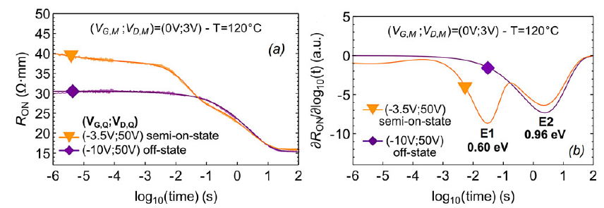
recovery traces reveal a larger current collapse for semi-on state stress as opposed to off-state stress. Right: Deep level drain current spectroscopy shows an additional defect state which is not present in the off-state degradation which serves as evidence for a hot carrier related mechanism
(from [68]).


