This chapter discusses the most important experimental aspects to obtain the macroscopically observed  drift of large-area devices under BTI stress as well as measurement techniques for single-defect characterization commonly observed on nano-scale devices.
Experimental characterization of devices requires both, knowledge about the structure and characteristics of the device under test, and the advantages and disadvantages inherent to the chosen measurement technique. Section 4.1 thus contains a discussion of four important measurement techniques for PBTI drift with respect to their applicability to GaN MIS-HEMTs and their potential to extract intrinsic defect parameters from the obtained results.
To be able to extrapolate lifetimes based on voltage or temperature accelerated measurements, or simply to optimize recipes to improve a certain technology, it is mandatory to obtain a deeper physical understanding of the involved mechanisms. Thus another important requirement is the ability to extract intrinsic defect parameters from the obtained data.
In a best case scenario, specific defect candidates can then be identified by comparing the results to first principle simulations [56, 57], microscopic methods like TEM [79], STM [80] or AFM [81] and physical methods like EDMR [82, 83] or ESR [84, 85]. However, many of those methods cannot be applied to fully processed devices or require special treatment of the sample, which makes a straight-forward comparison between the measurements complicated.
Because of the high density of surface defects in GaN, large devices will always contain the simultaneous response of a huge number of defects. For example, in a GaN device with a surface defect density of about  1/cm2 and an active area of 10 µm2, already
  defects will be active. A promising method to identify the microscopic nature of the defects responsible for the drift is single defect characterization which has already been demonstrated for silicon technology [86]. Therefore in Section 4.2, methods
to enable single defect measurements in GaN devices are outlined.
defects will be active. A promising method to identify the microscopic nature of the defects responsible for the drift is single defect characterization which has already been demonstrated for silicon technology [86]. Therefore in Section 4.2, methods
to enable single defect measurements in GaN devices are outlined.
In this section, a brief introduction for the measurement of drifts using four different well-established methods is given. The focus thereby lies on the discussion of these methods in the context of PBTI in GaN MIS-HEMTs [65]. Although the pros and cons of these methods are in
principle valid for other technologies too, their impact on the actual results can be significantly different depending on the specific context. A more general discussion on measurement methods for BTI can be found in [87–89].
The most straightforward way to measure the transient drift is to record two or more successive  or CV characteristics. The resulting hysteresis is then directly proportional to the number of trapped charges [74, 90, 91]. This method has several severe drawbacks for the extraction of the electrical response of the defects. The first one is that the hysteresis will be a function of the sweep rate, the minimum and maximum bias and the initial sweep direction
(up-sweep first vs. down-sweep first) [92, 93]. In addition, hysteresis measurements mix up the effects of bias acceleration with the influence of stress and recovery
times.
or CV characteristics. The resulting hysteresis is then directly proportional to the number of trapped charges [74, 90, 91]. This method has several severe drawbacks for the extraction of the electrical response of the defects. The first one is that the hysteresis will be a function of the sweep rate, the minimum and maximum bias and the initial sweep direction
(up-sweep first vs. down-sweep first) [92, 93]. In addition, hysteresis measurements mix up the effects of bias acceleration with the influence of stress and recovery
times.
Even though characteristics can be recorded down to the nanosecond regime with specialized equipment, the minimum sweep times available for standard parameter analyzers are limited to milliseconds. For PBTI in GaN, this poses ans additional complication because of the very broad range of capture and emission
times and the large density of defects. Defects being much faster than the sweep rate will cause an apparent dispersion of the characteristics. This can easily lead to misinterpretations of the obtained results, for example as  degradation. The separation of all these influences can be challenging, so the hysteresis method must be used with utmost caution for the extraction of intrinsic BTI defect parameters in GaN [94].
In the case of photo-assisted capacitance methods, for a wavelength above the AlGaN bandgap, the trap occupancy depends on the non-equilibrium concentrations of electrons or holes generated [95]. The defect response in this case is obfuscated because of the absence of holes in regular operating conditions and the unknown distribution of electrons and holes at the interface. For the defect properties obtained by photo-ionization experiments with below bandgap light, additional care has to be taken because of the Franck-Condon shift between the optical and thermal energies [96].
The conductance-frequency ( ) method has been used extensively to characterize interface defects in Si/SiO2 structures [97]. There are, however, two major problems when this method should be applied to GaN/AlGaN stacks. The first one is that like all
other capacitance based methods, it relies on an evaluation of a small signal excitation around a quasi-constant operating point. As all PBTI experiments show, this constant operating point cannot be established at forward bias conditions because of the ongoing drift. The second main difference is the response of the barrier. The conductivity of the barrier is a function of the applied forward bias, thus the measured changes in the conductivity always represent a superposition of the response of the barrier and the defects [93]. A detailed discussion on the limitations of the method in GaN MIS-HEMT structures can be found in [44].
) method has been used extensively to characterize interface defects in Si/SiO2 structures [97]. There are, however, two major problems when this method should be applied to GaN/AlGaN stacks. The first one is that like all
other capacitance based methods, it relies on an evaluation of a small signal excitation around a quasi-constant operating point. As all PBTI experiments show, this constant operating point cannot be established at forward bias conditions because of the ongoing drift. The second main difference is the response of the barrier. The conductivity of the barrier is a function of the applied forward bias, thus the measured changes in the conductivity always represent a superposition of the response of the barrier and the defects [93]. A detailed discussion on the limitations of the method in GaN MIS-HEMT structures can be found in [44].
Although the method is not very well suited fur MIS-HEMTs, it can still be applied to regular MOSFET devices where the electron channel is in contact with the III-N interface [93, 98]. Still, problems in the large-signal stability of the devices during characterization can lead to sweep-rate dependent conductance values [44].
A well-established method to obtain the threshold voltage shift following BTI stress is the MSM method. The idea is to measure the initial threshold voltage  of a device, apply stress to the device at elevated bias conditions and temperatures for some time and after that measure again. The threshold voltage shift can then be simply calculated as
  .
.
There are, however, two shortcomings to this approach. The first one, shared with all other methods which require a mapping from the drain current to  , is the required of the “fresh” device, which in general depends on the extraction method used on the transfer characteristics of the device [88]. Additionally, the initial characterization can already impose significant BTI stress if the response time of defects around is sufficiently small, as is the case for the devices studied here.
The second problem is the measurement delay  between the stress phases. As pointed out by Ershov in 2003, even for the comparably stable silicon technology there is a significant gap between the number of trapped charges between two subsequent stress cycles due to the delay [99]. This clearly demonstrates that the assumption of having a constant trap occupancy (i.e. no recovery) during the measurement of is not fulfilled.
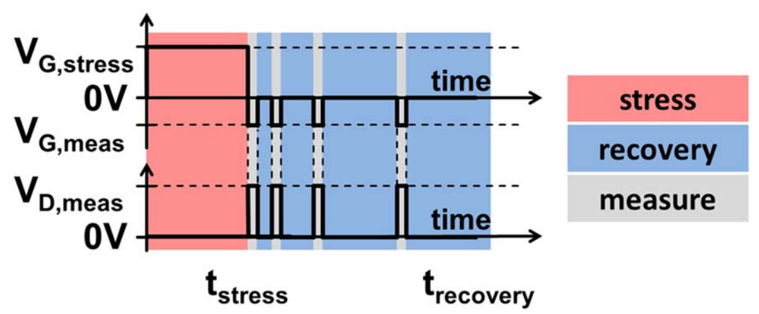
In the traditional MSM schemes, the stress phases are only interrupted as briefly as possible to record the degraded values of . The recorded stress data can therefore only contain information about charge capture events. Naturally, information about the recovery of defects cannot be obtained with these measurements. Instead of the short interruptions for measurements, in eMSM measurements a defined recovery phase spanning up to several decades in time is added between subsequent stress phases [100]. If the stress times between two phases are chosen to increase exponentially,
the influence of the recovery phase typically can be neglected if the total degradation is sufficiently small [101].
 of the pulse generator was used to record the transient drain currents (from [65]).
A typical eMSM setup which has been used to record the drift in Section 7.1.2 can be seen in Figure 4.1. There are, however, some fundamental
drawbacks of this method. Similar to the traditional MSM method, problems arise with the determination of 
 , the delay times between the different phases, and the amount of degradation imposed by the initial characterization. The other main drawback of this method is the insertion of the short measurement pulses during stress or recovery which potentially leads to a variety of unwanted side-effects like
accelerated recovery or additional responses from other defects due to the characterization. This error builds up over time and systematically underestimates the measured degradation.
, the delay times between the different phases, and the amount of degradation imposed by the initial characterization. The other main drawback of this method is the insertion of the short measurement pulses during stress or recovery which potentially leads to a variety of unwanted side-effects like
accelerated recovery or additional responses from other defects due to the characterization. This error builds up over time and systematically underestimates the measured degradation.
The distinct measurement pulses (see grey areas in Figure 4.1 (left)) are usually a consequence of the available measurement resolution of the ADC. This is because the available voltage resolution is determined by the current
resolution of the setup, the noise level and the transconductance of the device at the readout voltage. The trade-off between these those three parameters therefore sometimes requires to chose different readout voltages for the measurements and the biases applied for recovery.


(from [101]). degradation. The switches can be replaced by programmable voltage sources, offering the possibility to also conduct OTF measurements. The full-scale current and thus the measurement resolution can be set by using different values for  .
.
The steep subthreshold slope together with the very large PBTI drifts observed in GaN/AlGaN MIS-HEMTs can lead to situations where the amount of degradation exceeds the dynamic range spanned between the readout voltage and complete turn-off of the device. This either requires an adaption of the
measurement bias between the stress pulses or another type of setup using constant current regulation as shown in the left picture of Figure 4.2 [101]. The benefit of such a solution is that measurement resolution is only limited by the resolution of the data acquisition device for the gate voltage range of the device. The downside is that a constant drain current instead of a constant gate
bias is set during recovery. The consequence is that the applied gate bias changes with recovery which complicates the analysis of voltage acceleration of BTI. Furthermore, since the characterization is only a single-point measurement, dispersion effects in the characteristics due to HCD or current collapse will falsely be accounted as BTI drift. Another problem if the measurements are conducted in wafer probers is that a loss of contact or short-cuts between source and drain of the device will cause a full-scale gate bias as the desired drain current cannot be
regulated any more. This potentially induces additional unwanted BTI stress to the gate or may even damage the device.
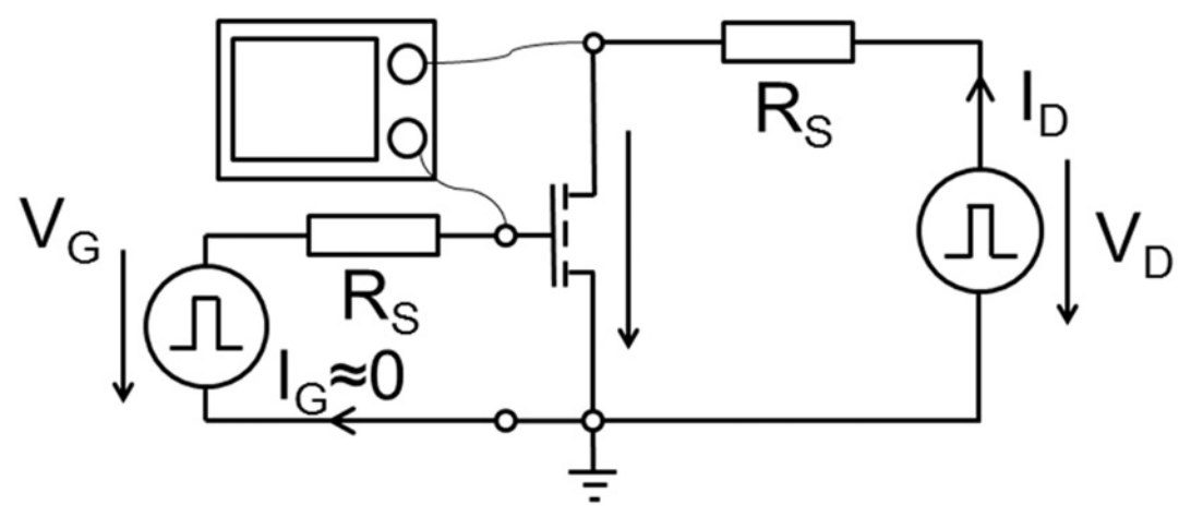
The right picture in Figure 4.2 shows the operation principle of the TMI, which is an instrument specifically designed by the Institute for Microelectronics to conduct reliability measurements [AGJ3, AGJ4][102]. The current-voltage converter ensures that the source potential
on the device is pinned to zero independently of the drain current. The measurement resolution can be chosen by selecting a full-scale drain current  . Together with the full scale voltage
  of the data acquisition unit, the required measurement resistor is calculated as
  . Note that the voltage switches for stress and recovery are actually programmable voltage sources allowing a much faster switching between the bias levels compared to physical switches. The main benefits of the TMI are the constant bias conditions during stress and recovery, very fast and low-noise
operation and the possibility to conduct OTF measurements.
. Note that the voltage switches for stress and recovery are actually programmable voltage sources allowing a much faster switching between the bias levels compared to physical switches. The main benefits of the TMI are the constant bias conditions during stress and recovery, very fast and low-noise
operation and the possibility to conduct OTF measurements.
One method which was introduced to overcome the limitations of the MSM techniques due to the measurement delay after stress is the OTF measurement [103, 104]. In these measurements, the drain current or the gate capacitance is monitored continuously across stress and recovery conditions. Therefore this method is particularly well suited for measurements where the device can be stressed and
monitored within similar bias ranges. If the device is operated in the linear regime, the drain current  can be mapped to using the initial threshold voltage and the corresponding drain current
  [105].
A more elaborate technique uses a small-signal modulation of the gate voltage around the current value to monitor the transconductance. These values are subsequently used calculate the BTI drift [103]. Although there is no measurement delay between stress and recovery, the intrinsic delay of the setup limits the minimum recordable stress time. Another intrinsic error stems from the fact that a characterization of the fresh device also needs to be conducted for stress conditions. This induces a certain amount of degradation to the device which eventually leads to an apparent dispersion and an overestimation of the stress during subsequent measurements.


