This chapter investigates the fundamental properties of gallium nitride-based devices. It starts with an overview on the crystal structure and fundamental properties of the available group-III nitrides being gallium nitride, aluminium nitride, and indium nitride. In Section 2.2, essential material parameters for electrical device simulation and the consequences of the electrical polarization in strained and unstrained nitrides are reviewed. The last section of this chapter starts with a discussion about the physics behind the formation of the 2DEG in GaN/AlGaN heterostructures. Afterwards, the fundamental design concepts of different normally-on and normally-off transistors are reviewed.
Group-III nitrides generally can crystallize in three different structures. The most important one is the hexagonal wurtzite structure being the thermodynamically stable structure at room temperature [7, 10, 11]. The second form is the zinc blende structure which can be stabilized on cubic substrates like Si, SiC or GaAs on the {0 1 1} crystal plane [12–14]. The rock salt structure can only be formed at high pressures and has so far only been investigated in fundamental research in material science and theoretically using ab-initio calculations.
Since the hexagonal structure is the thermodynamically stable form for all III-N semiconductors and most commonly used in fabrication, the other two forms are not going to be discussed throughout the remainder of this thesis. Consequently, all material parameters presented in this chapter and the results and conclusions presented throughout this work refer to wurtzite GaN.
As can be seen in Figure 2.1, the wurtzite crystal structure is formed by two interpenetrating hexagonal closed-packed sublattices for each of the atom types. Due to the hexagonal structure of the unit cells, it is
described by two lattice constants,  for the in-plane direction and
  for the perpendicular direction (i.e., the distance between two planes). The offset between the cells of metal and nitride ions in c-direction is
  . Another important property of III-N materials is the lack of an inversion plane perpendicular to the c-axis. This causes two different forms of the crystal, one terminating with the metal ions being in plane as in Figure 2.1 and one with the nitrogen ions on top. These two forms are usually referred to as Ga-face and N-face GaN in literature. The gallium atoms in Figure 2.1 can be replaced by other metals such as Al or In, forming the other two important III-N materials, AlN and InN [7, 11].
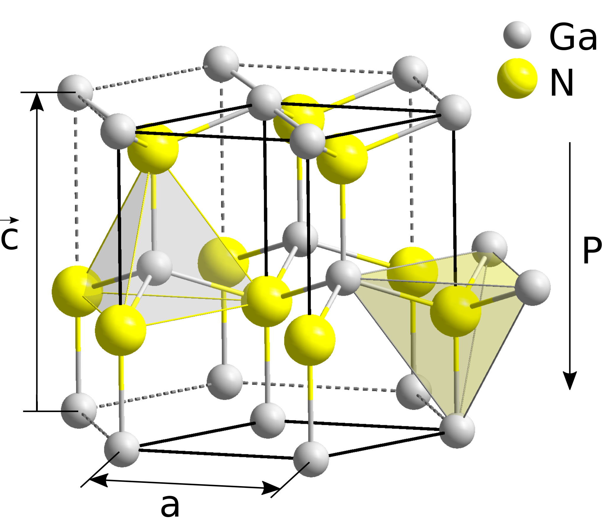
in along c-direction. The separation between the two lattices along the c-axis causes a spontaneous electrical polarization pointing from the metal to the nitrogen atom (from [15]).
Because of the distance between nitrogen (cation) and metal (anion), all nitride compound semiconductors show spontaneous and piezoelectric polarization. The importance of the metal-face and N-face crystals lies in the direction of the polarization which is always pointing from the anion to the cation across the c-direction. A thorough discussion of the polarization effects in nitrides is given in Section 2.2.4.
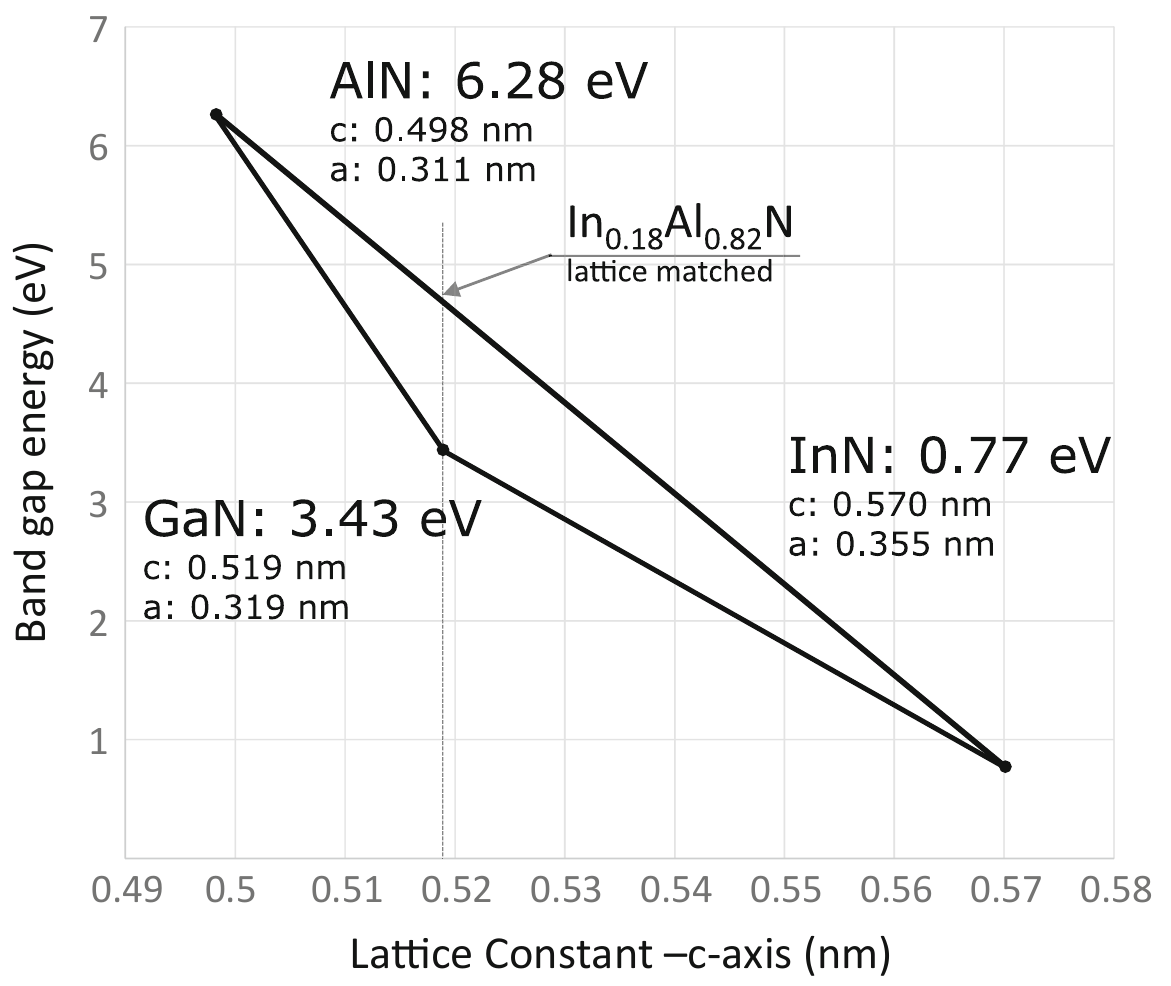
Like in many other III-V compound semiconductors, one key feature of many GaN based devices relies upon the formation of heterostructures enabled by the ability to engineer the bandgap and – if applicable – the polarization of the materials by using ternary alloys. In the case of group III nitrides, an
unprecedentedly large range of energies is available, ranging from about 0.77 eV for InN to 6.28 eV for AlN [2]. The mismatch in the lattice constants between the substrate (usually GaN) and the pseudomorphically (i.e.
grown without lattice relaxation) grown alloy on top thereby induces mechanical strain which causes an additional piezoelectric polarization in the strained layer. The relationship between the bandgap energies and the lattice constant is given in Figure 2.2.
The choice of substrate materials for GaN based devices strongly depends on the device architecture. Up to date, most efforts in GaN epitaxy concentrate on foreign substrates like Si, SiC, and sapphire [16, 17] because of the absence of native substrates. The foreign substrates thereby introduce mechanical strain due to mismatches in the lattice constants and thermal expansion coefficients of the different materials. The best available substrate material is SiC with a lattice mismatch of only 3.1 % and a linear expansion coefficient of 4.4 × 10⁻⁶/K as compared to 5.6 × 10⁻⁶/K for GaN. The high thermal conductivity of the SiC substrate additionally allows for efficient heat dissipation in power devices. Nonetheless, the very high price compared to silicon wafers limits the usage of SiC as a substrate material.
Despite having the largest lattice constant mismatch (−17 %) and the largest mismatch of the thermal expansion coefficient (2.6 × 10⁻⁶/K) of all common foreign substrates compared to GaN, the wide range of available sizes, lower costs and its compatibility to existing fabrication processes
makes silicon a very attractive base substrate for GaN devices. Special strain management techniques and nucleation layers are needed to prevent crack formation and help to obtain low dislocation densities on the order of  1/cm2 [17].
Sapphire as a base material suffers from similar problems as silicon regarding mechanical strain and crack formation [18]. The particularly low thermal conductivity of  can be mitigated by flip-chip bonding of the devices onto a material with high thermal conductivity [19]. Sapphire is especially attractive for high-frequency devices because it is naturally insulating and thus has a much higher resistivity
compared to silicon wafers.
can be mitigated by flip-chip bonding of the devices onto a material with high thermal conductivity [19]. Sapphire is especially attractive for high-frequency devices because it is naturally insulating and thus has a much higher resistivity
compared to silicon wafers.
Native GaN substrates currently can be grown by different techniques up to sizes of 3 ” [20]. Superior dislocation densities, typically two to four orders of magnitude better than films grown on the other substrate materials, help to lower leakage currents and raise the breakdown voltage of the devices. They also enable the design of vertical power devices which obviously cannot be manufactured on foreign substrates. Despite many improvements during the last years regarding cost-effective large-scale production of high-quality native GaN wavers, many challenges still need to be overcome. Native substrates are thus by far the most expensive choice among all the discussed materials.

