Despite some GaN HEMTs and MIS-HEMTs being already commercially available, there are still concerns regarding their reliability. Especially charge trapping phenomena prevent researchers and engineers from a further exploitation of the theoretical capabilities of the material system.
This chapter starts with an introduction of the most common defects present in GaN/AlGaN devices. Afterwards, the mechanisms and the state of current research regarding the three major reliability issues, all of them caused by charge trapping, are discussed. These are drain current or  dispersion which are usually referred to as current collapse,
  drift or NBTI/PBTI and hot carrier related effects.
Due to a variety of reasons, mainly the lack of native substrates for epitaxy and other growth-related issues like thermally induced mechanical stress, the intrinsic defect density in GaN technology is higher as compared to silicon. Moreover, the used substrate, as well as growth technology and processing, greatly influence the type of the observed defects as well as their densities. Due to that reason, the undoped, as-grown bulk material is usually referred to as unintentionally doped (UID) GaN which commonly appears to be an n-type semiconductor.
Usually, the observed defects are categorized into four different classes:
• Native Defects are present in bulk GaN due to crystallographic imperfections. Based on the type of defect, these can be missing Ga or N atoms called vacancies ( and
and  ), atoms at the site of their counterpart called antisites (
 and
and  ), or atoms present in the space between the crystal sites called interstitials (
 and
and  ).
).
• Impurities can be brought into the structure intentionally as doping (Mg, Fe, C, Si) or unintentionally via residuals in the reactor or during processing via the atmosphere (H, O) or precursor gases (C, H). The species often substitute one type of lattice atom and subsequently creates unwanted energy levels within the bandgap. On a side note, the presence of dopants always distorts the crystal lattice and can thus potentially increase the density of native defects.
• Surface defects are of special importance in GaN due to its polar nature. At the interface between crystalline and amorphous materials, the periodicity of the lattice stops abruptly, leading to the formation of a multitude of dangling bonds and other electrically active defects. In this case, due to the polarization charges, this trend is even more pronounced as the polarization charges forming the 2DEG are widely thought to be compensated by donor states at the surface (see Section 2.3.1).
• Dislocations are extended defects which are primarily formed due to the imperfect surface on the substrate or mechanical stress induced by thermal stress or a mismatch in the lattice constants between two materials (various types of dislocations or stacking faults). Other types of extended defects are formed by molecules of different species (usually oxidized impurities) which tend to form complexes with dislocations, obscuring their theoretically predicted electrical response.
There is a large variety of literature dealing with the identification, classification and electrical characterization of point defects in bulk GaN and AlGaN. This section briefly summarizes the most common defect levels of native defects and impurities in bulk GaN. A more detailed introduction into the defect physics of nitride semiconductors is given in Chapter 4 in [7], Chapter 9 in [54], and [55].
First principle simulations using DFT combined with quantum molecular dynamics were used to provide the formation energies and electronic structure of a large variety of defects [56, 57]. There is a considerable spread in the provided transition levels, mostly due to the type of applied bandgap correction and the used DFT functionals. Another problem is that often unstrained crystal structures are used for the calculations, introducing additional errors.
The results of the first principle simulations are then compared to measurements by a multitude of different techniques. The most important one among the different methods is DLTS [58, 59] as well as its variation using optical excitation of defects [59, 60]. Other commonly used methods are photoluminescence spectroscopy [54, 61], scanning capacitance microscopy and positron annihilation spectroscopy [7].
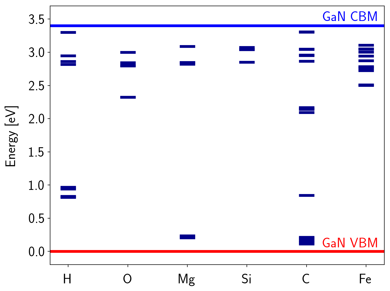
Despite considerable efforts to attribute defect levels within the GaN bandgap to certain kind of defects, only some of them could be assigned with sufficient confidence. This is partly due to measurement uncertainties or systematic errors introduced by the particular method used. A good summary of the most common defect levels observed in GaN and their ascribed types is given in Figures 3.1 and 3.2. The corresponding Arrhenius plots containing the capture cross sections of the various defects can be found in [55].
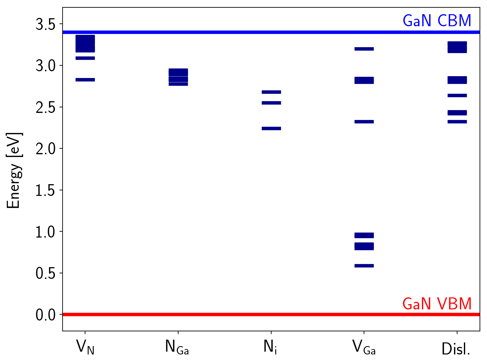
), the nitrogen antisite (), the nitrogen interstitial (), the gallium vacancy (), and various extended dislocation type defects.
In the case of bulk AlGaN, the same structural defects in general appear with another activation energy as compared to GaN [62]. This is simply justified by the fact that even if the same ionization energies to the vacuum level are assumed for a certain defect, the energy differnces to the conduction and valence band edges have to change with the alloy composition. On the other hand, there is evidence for other defect levels appearing in AlGaN which are either related to Al or other defects that are probably outside the energy gap in the case of GaN [63, 64]. Finally, some additional defects have been found that only seem to appear on fully processed devices [62, 63].
Of all the defects presented in Figure 3.1, the dominating intrinsic defect is thought to be the nitrogen-vacancy together with its complexes. The  -type conduction present in as-grown GaN samples is usually attributed to this defect because of its shallow donor behavior. The most prominently investigated impurities are carbon which is commonly used for co-doping to obtain a semi-insulating buffer as well as magnesium which is mainly used as an
acceptor in
-type conduction present in as-grown GaN samples is usually attributed to this defect because of its shallow donor behavior. The most prominently investigated impurities are carbon which is commonly used for co-doping to obtain a semi-insulating buffer as well as magnesium which is mainly used as an
acceptor in  -type GaN. The interest in investigating hydrogen as an impurity is primarily due to its role in forming complexes with other defects creating deep donors as well as deep states around mid-gap [55].
It has to be noted that the vast number of different electrically active states within the bandgap of GaN/AlGaN devices obfuscates the allocation of an electrical response to a certain microscopic defect. The high intrinsic defect densities together with co-doping schemes introduced to obtain semi-insulating buffer materials further complicate correct defect parameter extraction. The polarization field in the AlGaN barrier poses additional problems in the interpretation of measurement data. This is probably the reason why reported parameter values for the same defects show a significant spread throughout the literature.
Trapping in interface defects are one of the major mechanisms affecting the performance of GaN/AlGaN HEMTs. Unlike in silicon devices, where usually minority carriers controlled by doping form an inversion channel, in HEMTs the defect states at the surface are necessary for the formation of the 2DEG at the channel interface due to the commonly accepted surface donor model as explained in Section 2.3.1. On top of that, the tensile strain formed in the AlGaN layer introduces additional dislocations to the material.
In the case of Schottky HEMTs, electron trapping at the surface is usually reported as current collapse or historically also as “virtual gate” effect. The electrons trapped at the surface of the transistor access regions decrease the surface potential and thus weaken the 2DEG (see also Section 3.2.1). It has later been found that passivating this interface with SiN or other insulating materials helps to decrease the current collapse [36–38].
When creating MIS-HEMTs, the interface between AlGaN and the insulator is not just present at the access regions of the transistor but also underneath the gate. This makes the same surface donor states much more accessible for electrons, especially when applying a positive bias to the gate, see Section 3.2.2.
In general, the structure and the electrical response of the surface donors is still a matter of debate [6, 44, 65]. The impact of different insulator materials on the electrical response of the surface donors is, if at all, only weakly understood up to now either. This is partly because of the lack of a stable native oxide, creating a relatively low-quality
oxide semiconductor interface and partly to the sheer number of active defects which has to be in the order of the sheet carrier density of the channel ( ) [66].

