During the last four decades, the world’s total electricity consumption has dramatically increased from 6.1 PWh in 1973 up to 24.3 PWh in 2015, which is an overall increase of almost 400 % [1]. Despite considerable efforts to promote renewable energy sources (hydro, wind, solar, geothermal and others) during the past two decades, their total market share has increased only marginally from 21.5 % to 23.1 %. At the same time, the amount of electricity in the global energy consumption has almost doubled from 9.4 % to 18.5 %.
If the international goals to limit carbon dioxide emissions should be met, the trend to use electricity as a primary energy source will ever increase as sectors as for example individual and public transport are going to be more and more electrified in the near future. To significantly increase the amount of electricity from renewable sources, not only the production and consumption of electricity but also the conversion efficiency is going to play a crucial role in the future.
For that reason, there is an ever growing interest in creating more efficient power semiconductor devices, with a special focus on wide-bandgap materials like GaN and SiC because their fundamental material properties are far superior to silicon. To obtain a widespread acceptance of such devices, several technological issues have to be solved. Most importantly, the reliability of these devices is still a major concern in present technologies. For many device concepts, charge trapping in defects is a severe performance limiting factor which prevents manufacturers to actually exploit the superior material properties of SiC and especially GaN.
This chapter briefly explores the reasons for the ever-growing interest in wide-bandgap semiconductors by comparing them to other materials using various figures of merit. The comparison will mainly focus on power applications being one of the most promising applications in the future. The second part holds a brief motivation for this work, followed by a short description of the content and the focus of the different chapters.
Power semiconductor devices are typically used to control the electrical power flow in switching mode power supplies. For that purpose, they are only operated under two different conditions, the on-state and the off-state. Unlike ideal switches which conduct current without any losses in the on-state and block any voltage in the off-state, power semiconductor devices consume energy in both of these states and can only block finite voltages before breaking down. In addition, real power switches also consume energy for switching between the on- and off-state. To make power switches as efficient as possible, all of these three contributions to the overall losses need to be minimized.
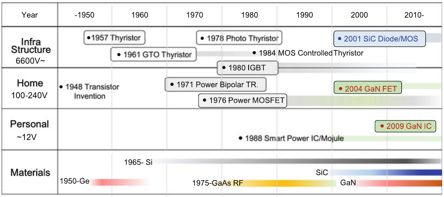
Power conversion systems are used in a broad range of applications with nominal powers ranging from several watts (e.g., chargers for consumer electronics) to several gigawatts (e.g., high-voltage transmission systems for offshore wind parks). The applications are usually split into layers based on the required voltage range. The three major application layers, infrastructure for large voltages in the kV range, home for domestic power applications, and personal for integrated power conversion systems with low voltages and high currents, are shown in Figure 1.1. The personal layer has emerged recently, as the operating voltages of highly integrated circuits were scaled to values as low as 1 V for hundreds of millions of transistors. The usual application for this layer is a down-step converter from the battery voltage in a mobile device with tens of amperes of output current.
To understand the recent interest in wide-bandgap semiconductors, the main parameters of power devices and the trade-offs between them need to be discussed. The most important parameters of a power switching device are summarized as
• on-resistance  ,
,
• nominal current,
• breakdown voltage  ,
,
• switching capacitance.
Since all the parameters mentioned above strongly depend on the fundamental device concept and the device geometry, a fair comparison of different materials is not possible. The general suitability of different semiconductor materials for power applications should instead be calculated based on the fundamental electrical properties rather than device specific parameters. In the following, two important figures of merit for power semiconductors, namely BFoM and JFoM are introduced and will later be used to compare different wide-bandgap semiconductors to silicon.
For any material used in power devices, the specific on resistance as the main contributor to the conduction losses should be kept as low as possible with the breakdown voltage being as high as possible. Baliga’s figure of merit combines these two parameters into a single figure of merit, which is the specific power
density a given material can theoretically withstand. It is calculated with the permittivity  of the material, the electron or hole mobility
  , and the critical electric field strength for material breakdown
  [3, 4].
Note that for a given material, a higher numbers means a lower specific on resistance and thus less conduction losses for a given technology. For unipolar devices in the one-dimensional limit, BFoM connects the specific on resistance of the device  to the breakdown voltage of the device.
In modern switching mode power supplies, switching losses often make up for the largest contribution to the overall losses. Additionally, modern mobile base stations and radar applications requires power amplifiers in the microwave and millimeter-wave frequency range. For high-frequency applications, a basic
trade-off between breakdown voltage and transit frequency is needed. This trade-off is reflected by JFoM [5]. In a first order approximation, the maximum transit frequency  of carriers through a MOSFET channel is given by the channel length
  and the saturation velocity for electrons or holes
  .
.
Considering a uniform field across the channel, the breakdown voltage can easily be calculated from the critical field strength as  . The product of these two parameters becomes constant and independent of the channel length. This constant is usually referred to as Johnson’s limit or JFoM.
The interest in wide-bandgap materials can be understood best if their most important material properties are compared to those of other common semiconductors. In Table 1.1, the most fundamental material properties of common wide-bandgap semiconductors are listed together with those of silicon and GaAs [2, 6–8]. Both figures of merit, BFoM for the conduction losses and JFoM for the switching losses show a large advantage for the wide-bandgap semiconductors when compared to Si or GaAs. On top of that, the superior thermal conductivities offer the ability to ease some of the problems regarding the thermal design of devices.
| Parameter | Si | GaAs | GaN | AlN | SiC(6H) | SiC(4H) | |
 |
[eV] | 1.12 | 1.42 | 3.39 | 6.2 | 3.02 | 3.26 |
|
[1] | 11.7 | 10.9 | 8.9 | 8.5 | 10 | 9.7 |
 |
[cm2/(V s)] | 1500 | 8500 | 1000 | 300 | 900 | 400 |
|
[MV/cm] | 0.3 | 0.55 | 3-5 | 1.2-1.8 | 3 | 3 |
 |
[ cm/s] cm/s] |
1 | 1.2 | 2.5 | 3.7 | 2 | 2 |
 |
[W/(cm K)] | 1.5 | 0.46 | 2.1 | 2.85 | 2.3-4.9 | 2.3-4.9 |
| BFoM | [TW/cm2] | 0.42 | 13.6 | 504 | 7.62 | 215 | 92.8 |
| JFoM | [THz V] | 0.48 | 1.05 | 15.9 | 8.24 | 9.55 | 9.55 |
The improved critical field also helps to overcome the scaling limit for power conversion devices made of silicon. Table 1.2 shows well-known scaling rules for essential parameters in silicon MOSFET technology for a scaling factor of  . Assuming a constant voltage design, the larger values of the critical field in wide-bandgap semiconductors offer quite some margin for further miniaturization. Note that the breakdown voltage scales linearly, while other key chip parameters like area, switching losses, and cost scale quadratically with the
applied scaling factor.
. Assuming a constant voltage design, the larger values of the critical field in wide-bandgap semiconductors offer quite some margin for further miniaturization. Note that the breakdown voltage scales linearly, while other key chip parameters like area, switching losses, and cost scale quadratically with the
applied scaling factor.
| scaling factor: |
|
|
 |
|
|
| chip area |  |
| chip cost | |
| capacitance | |
| switching loss | |
. If the wide-bandagap devices are designed for the same voltage and current rating, an improvement of a factor of around 100 in chip area and switching losses can be obtained theoretically.
The ratios between the breakdown fields of GaN or SiC and Si thus allow reducing chip area and switching losses by a factor of 100 while keeping roughly the same voltage and current ratings (neglecting thermal design). Of course, this is just a theoretical value as factors like the matureness of the technology, fabrication cost or process compatibility are often limiting factors preventing technologies from a broader market adoption.
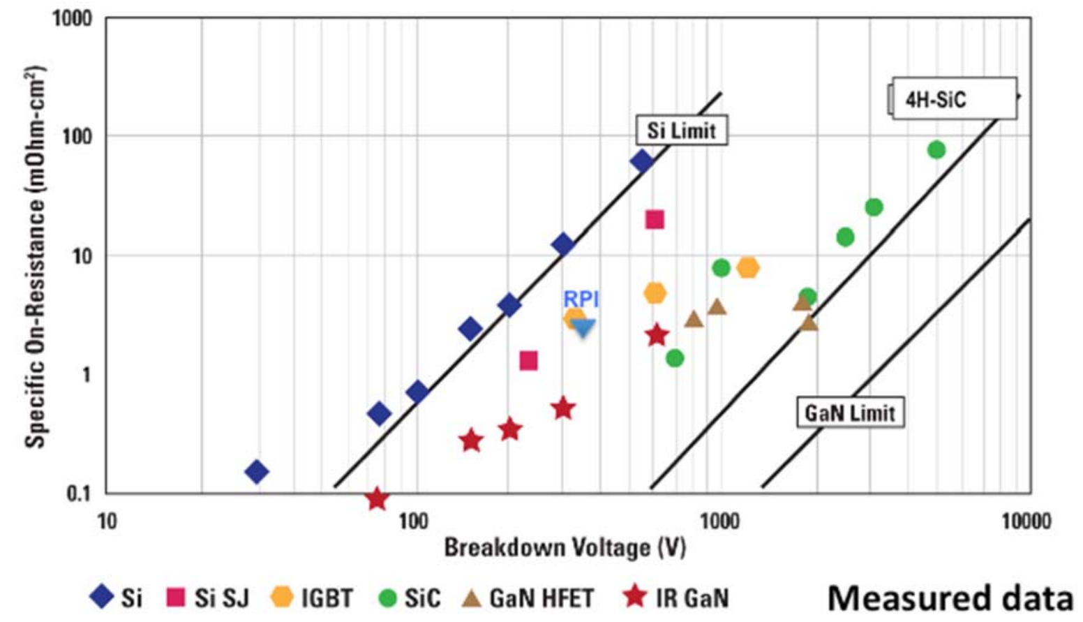
To see the current status of realized GaN and SiC devices compared to silicon power devices, in Figure 1.2 the values of versus the breakdown voltage across different state of the art device concepts and technologies are shown [9]. Although the theoretical MOSFET limit of silicon can be stretched by using different concepts like super-junction
transistors or IGBT, the GaN and SiC devices clearly outperform silicon devices despite being an immature technology.
Overall, wide-bandgap materials like GaN and SiC offer superior material properties, both for high-power and high-frequency operation. In the high-power regime, this allows for significant improvements regarding the energy efficiency and required chip area due to scaling. The improved high-frequency operation makes them ideal candidates for power amplifiers in the microwave and millimeter frequency regime. For applications in power switching, higher operating frequencies also allow to scale down passive components like transformers, capacitors or inductors. This helps to decrease costs for power conversion systems when using wide-bandgap semiconductors.


![(1.1) \begin{equation} \mathrm {BFoM} = \epso \epsr \mu _\mathrm {n,p}\Ec ^3\ [\si {\watt \per \metre \squared }] \eqlabel {intro:bfom} \end{equation}](images/image-9.svg)
![(1.2) \begin{equation} R_\mathrm {on,\Box } = \frac {4B_\mathrm {v}^2}{\epso \epsr \mu _\mathrm {n,p}\Ec ^3}\ [\si {\ohm \per \metre \squared }] \eqlabel {intro:ron} \end{equation}](images/image-12.svg)

