This section covers the most important material parameters for device simulation for all three group-III nitrides and their alloys. As many parameters used throughout the literature still show a significant amount of scatter, the set of parameters used by the device simulator Minimos-NT [21] for the simulations in the remainder of this work is listed and justified. A more detailed discussion of the electronic material parameters in GaN, AlN, InN and their alloys can be found in [7, 8, 22].
One of the most important electrical parameters defining semiconducting materials is their energy gap and the alignment of the conduction and valence band edges of the different materials to each other.
The dependence of the bandgap energy on the lattice temperature  is often described empirically by [7]
The alignment of different materials can be expressed in different ways. One of the most common ones is to use the electron affinity  , which in solid state physics is defined as the energy difference between the conduction band edge and the vacuum energy. In Minimos-NT [21], the energy alignment is expressed using offset energies relative to the valence band edge.
The band edges are then calculated as
, which in solid state physics is defined as the energy difference between the conduction band edge and the vacuum energy. In Minimos-NT [21], the energy alignment is expressed using offset energies relative to the valence band edge.
The band edges are then calculated as
| Parameter | GaN | AlN | InN | Ref. | |
 |
[eV] | 3.4 | 6.2 | 0.9 | [22] |
 |
[eV] | – | -1.12 | 0.58 | [22] |
 |
[meV/K] | 0.909 | 0.018 | 0.414 | [22] |
 |
[K] | 800 | 1462 | 454 | [22] |
 |
[1] | 1 | 1 | 1 | [8] |
 |
[1/ ] ] |
0.2 | 0.4 | 0.04 | [8, 22] |
 |
[1/] |
1.0 | 7.26 | 1.15 | [8] |
 |
[1] | 8.6 | 8.5 | 15.3 | [8, 23] |
Other important parameters are the relative permittivity of the materials and the effective carrier masses which are used to calculate the effective density of states by
with being the number of equivalent conduction band minima. The parameters used for the device simulations are listed in Table 2.1.
For drift-diffusion simulations, the most important material parameters are the carrier mobilities  and carrier saturation velocities
  . A simple power law is typically used to empirically describe the temperature dependence of the low field electron mobility
  .
.
Mobility reduction due to ionized impurity scattering for III-V semiconductors is often calculated using the empirical formula of Caughey and Thomas [24] with temperature dependent coefficients.
The temperature dependent parameters for the Caughey-Thomas equation are again calculated with simple power laws.
The high-field mobilities are calculated in dependence of the driving force  and the saturation velocity
  of the electrons using [21]
Because of their low mobilities, holes are of minor interest for transport in most GaN power devices. Therefore the hole mobilities are typically modeled by constant values. The transport parameters for the three binary nitrides are listed in Table 2.2. If some material parameters like the saturation velocity for holes and some of the mobility parameters cannot be determined for AlN and InN, the respective values of GaN are used.
| Parameter | GaN | AlN | InN | Ref. | |
 |
[cm2/(V s)] | 1405 | 683 | 10400 | [22, 25] |
 |
[1] | -2.85 | 0.8 | -3.7 | [22, 25] |
 |
[cm2/(V s)] | 80 | 29 | 500 | [22, 25] |
 |
[1] | -0.2 | -3.21 | 2.39 | [22, 25] |
 |
[1/cm3] | 7.78 × 10¹⁶ | 5 × 10¹⁷ | 3.4 × 10¹⁷ | [22, 25] |
 |
[1] | 1.3 | 1.21 | -0.33 | [22, 25] |
 |
[1] | 0.71 | -0.18 | 0.7 | [22, 25] |
 |
[1] | 0.31 | 0.31 | 0.31 | [25] |
 |
[1] | 1 | 0.45 | 1 | [22, 25] |
 |
[cm/s] | 2.5 × 10⁷ | 3.7 × 10⁷ | 5 × 10⁷ | [8, 22] |
 |
[cm/s] | 7 × 10⁶ | 7 × 10⁶ | 7 × 10⁶ | [8] |
 |
[cm2/(V s)] | 170 | 14 | 220 | [2, 8] |
The material parameters for ternary alloys like AlGaN or InGaN can usually be calculated by linear or quadratic interpolation of the respective binary compounds based on the alloy parameter  . For most of the parameters mentioned in Sections 2.2.1 and 2.2.2, the equation reads:
Here,  and
and  are the parameters of the binary compounds and
  is called bowing parameter. There are two exceptions to this rule, namely for the band energy offsets and the electron mobilities. If the ratios between conduction band offset and valence band offset is assumed to be constant over the whole composition range, for the energy offset the mixing equation reads [26]
while the effective low-field mobility is calculated by
Table 2.3 lists the bowing parameters for the different quantities used in the simulations for the two alloys AlGaN and InGaN.
| Parameter | AlGaN | InGaN | Ref. | |
|
[eV] | -1.33 | 1.4 | [8, 22] |
 |
[cm2/(V s)] | 40 | 1 × 10⁶ | [8] |
|
[cm/s] | −3.85 × 10⁷ | 0 | [8] |
|
[1] | 4.8 × 10⁻³ | 0 | [8] |
|
[1] | 0 | 0 | [25] |
As mentioned previously, all group-III nitrides show spontaneous and piezoelectric polarization because of the distance between the planes of the nitrogen and the metal ions in the crystal structure. The sign and magnitude of spontaneous polarization depend on the difference in electronegativity between the metal
and the nitride. For ternary alloys like AlGaN, the macroscopically observed polarization is a function of the alloy parameter between the two binary semiconductors. As can be seen in Figure 2.2, also the lattice constants  and
and  depend on the used alloy composition.
If for example a layer of AlGaN is grown pseudomorphically on top of an unstrained GaN buffer, the mismatch of the lattice constants cause tensile strain in the AlGaN layer, which induces an additional amount of piezoelectric polarization on top of the spontaneous polarization. A schematic picture of the different terms of polarizations present in a GaN/AlGaN heterostructure can be seen in Figure 2.3.

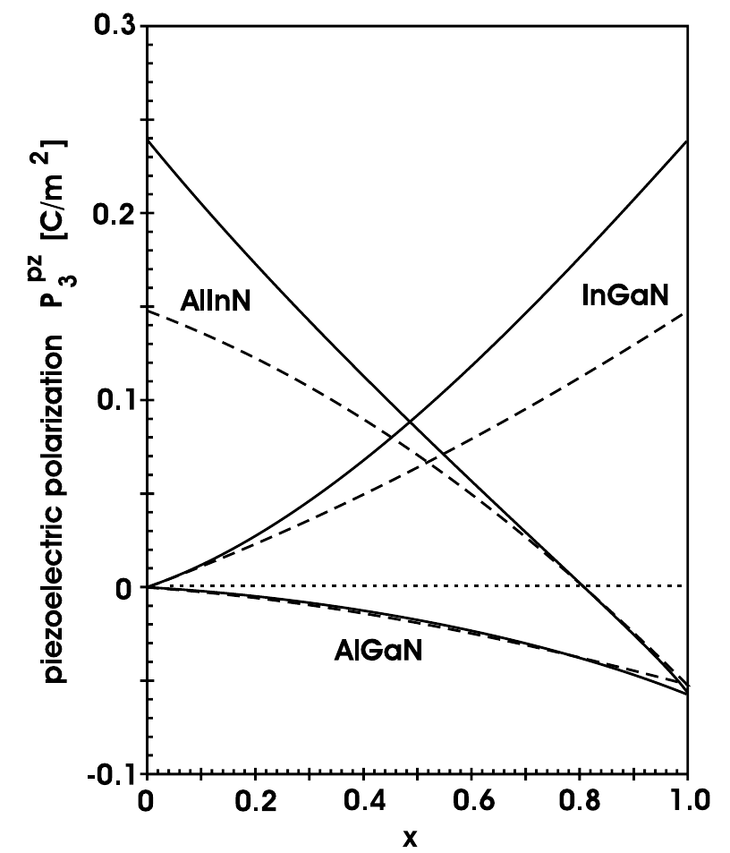
In Figure 2.4, the amount of spontaneous and piezoelectric polarization of different nitrides in dependence of their alloy composition can be seen. For the calculation of the piezoelectric polarization, the alloy is assumed to be grown on top of a relaxed GaN buffer. The dashed lines for the piezoelectric polarizations are calculated with a linear interpolation between the strain parameters of the binary compounds. Especially for highly strained layers containing large amounts of indium, the nonlinearities due to the strain should be taken into account (solid lines) [27].
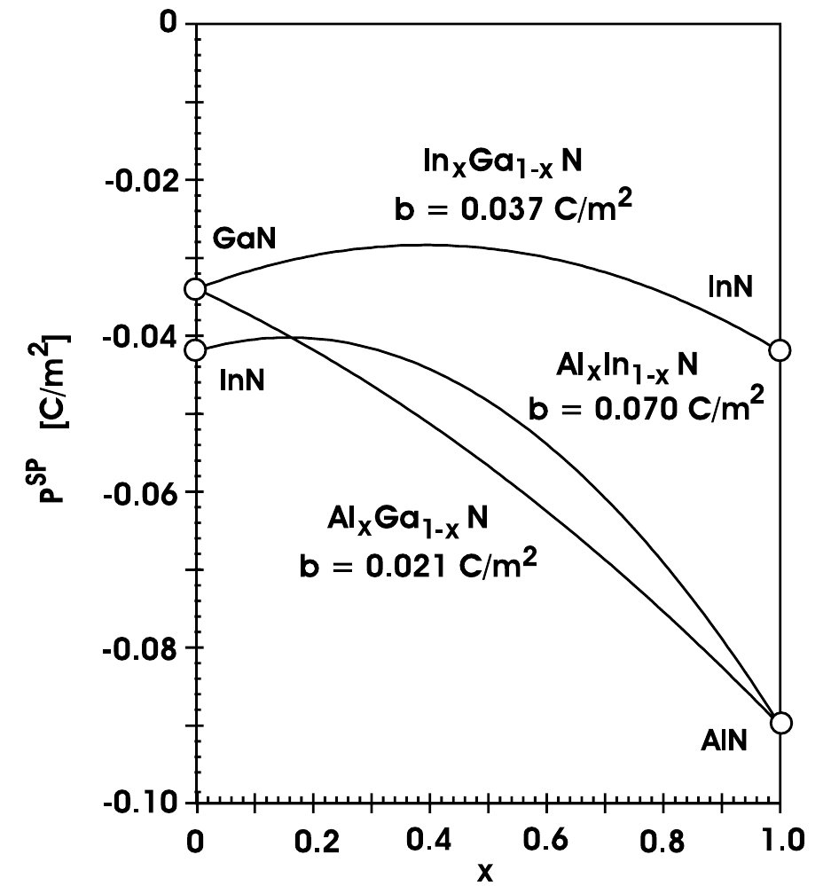
The values in Figure 2.4 for the spontaneous and piezoelectric polarizations for the most important binary and ternary alloys can be calculated in dependence of [27]:
The piezoelectric polarization obviously depends on the used buffer material. For weakly strained ternary alloys grown on an unstrained GaN buffer, the following equations hold [27]:
For highly strained InGaN and AlInN layers, the linear interpolation in (2.18)-(2.20) severely underestimates the amount of piezoelectric polarization (solid lines in Figure 2.4). A refined approach for the calculation in those cases can be found in [27]. The polarization-induced bound charge density can be calculated by taking the gradient of the total polarization in space.
As mentioned before, nitride compound semiconductors only have a polarization across the c-axis with its sign depending on the surface termination of the crystal surface (Ga-face or N-face). For the material interfaces in heterostructures as shown in Figure 2.3, the value of the polarization also jumps at the GaN/AlGaN interface because of the different values of spontaneous and piezoelectric polarization. The abrupt change of polarization across the c-direction thus causes fixed two-dimensional charge densities at these interfaces. For the GaN/AlGaN heterostructure the values read as:


