|
In the development of today's electronic devices, the simulation of processes and physical effects is key in the creation of competitive products. When electronic devices are simulated, the device structures have to be a realistic image of the actual devices. With the growing complexity of the structures and the difficulty of interactively defining their geometries, especially in three dimensions, development tools for the simulation of the whole process flow of the manufacturing process and the delivery of the final device have become necessary. Due to the growing demands, these process simulation tools, such as implantation, diffusion, deposition, and etching tools, are continually being improved.
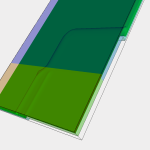
Etching and deposition change the topography of the surface of the wafer. Dealing with these resulting non-planar surfaces in three dimensions is essential in simulation. Easily describing these complex three-dimensional surfaces, a level set method is well suited. Therefore, a topography simulator with a level set kernel was developed. The development of the etching tools focused on a three-dimensional physical evaluation model for sacrificial etching and simultaneous etching of different materials with varying etch rates in a single simulation. A common aspect of both topics is THe coexistence of wide, very thin but broad regions of the attacked material, which made it necessary to expand etching from all directions in space, also expanding the resolution of the etcher. The handling of regionally different etch parameters was necessary for more material-etching. After the topography simulations are applied, the level set representation of the etched material has to be made applicable for the following simulation tools which work mainly on tetrahedral meshes. The level set representation is only a regional distribution of the distance function defined on an ortho product grid. Therefore, a back conversion to a tetrahedral grid is necessary. Currently the development focuses on this back conversion. First, the material front has to be extracted from the distribution. To reduce the complexity of the resulting structure, this surface has to be simplified. Afterwards, the already existing meshed input structure has to be cut with the extracted level set surface of the material front. Finally, the inside parts have to be joined to a tetrahedral representation.
|