|
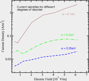
Organic semiconductor devices are assemblies of about 100nm thin polymer films exhibiting a certain degree of molecular disorder. These functional layers are constituted by van der Waals-bound, hence soft, lattices which are distorted by the Coulomb potentials of traversing electrons. The confined "polaronic" motion of charges with their corresponding lattice-distortions gives rise to a set of activated transport regimes ranging from incoherent thermally assisted tunneling to bandlike small polaron transport. The dispersive nature of these regimes is due to the loss of long-range order but not related to the system's chemistry. However, the interplay of the different charge-transfer mechanisms with specific properties of branched bonding and antibonding molecular wave functions is one of the most interesting open questions in the modeling of organic devices, since it can be utilized to govern the sample's electrical characteristics. The physical phenomena governing a device's electrical characteristics include charge injection and transport, exciton creation, and electron-vacancy recombination in an electric field of the order of 1 MV/cm. To study all processes simultaneously for electrons obeying the Pauli principle a 3-dimensional Kinetic Monte Carlo (KMC) Simulator has been implemented which bridges the gap between molecular dynamics (MD) and ensemble Monte Carlo (MC) techniques in the field of organic microelectronics. The MD method models the dynamics directly as a causal sequence of configurations derived from the particles' equations of motion. However, for large systems or complex energy landscapes the time-scale of MD is limited to nano- or even picoseconds. On the other hand, the phase-space traversal of classical MC techniques does not describe how the system evolves towards its steady state in a chronological sense. By assigning an individual time scale to each event, KMC enables a kinetic, rate-based description of the electron gases' (driven) dynamics. The simulator developed works with arbitrary electron and dopant-concentrations, space-charge accumulations and distributions, molecule-sizes, and heterojunctions including metal-contacts. A joint non-adiabatic transition rate rules events with time scales varying over several orders of magnitude. The simulations focus on the bulk and interface-effects in polycrystalline and amorphous zinc phthalocyanine (ZnPc) films in the weak-coupling regime. Since the charge flow strongly depends on interfaces and boundaries, Au/ZnPc/Au-devices are simulated in-situ. The main emphasis is placed on the numeric effects of varying carrier-concentrations and morphologies. Current-voltage characteristics for films up to a length of 140nm have been simulated.
|