Erasmus Langer
Siegfried Selberherr
Hajdin Ceric
Johann Cervenka
Siddhartha Dhar
Robert Entner
Wolfgang Gös
Klaus-Tibor Grasser
René Heinzl
Christian Hollauer
Stefan Holzer
Andreas Hössinger
Gerhard Karlowatz
Markus Karner
Hans Kosina
Ling Li
Gregor Meller
Mihail Nedjalkov
Alexandre Nentchev
Vassil Palankovski
Mahdi Pourfath
Philipp Schwaha
Alireza Sheikholeslami
Michael Spevak
Viktor Sverdlov
Oliver Triebl
Enzo Ungersboeck
Martin-Thomas Vasicek
Stanislav Vitanov
Martin Wagner
Wilfried Wessner
Robert Wittmann

Vassil Palankovski
Dipl.-Ing. Dr.techn.
palankovski(!at)iue.tuwien.ac.at
Biography:
Vassil Palankovski was born in Sofia, Bulgaria, in 1969. He received his diploma in electronics from the Technical University of Sofia in 1993. Afterwards he worked for three years in the telecommunications field. In March 1997, he joined the Institute for Microelectronics at the TU Wien, where he received the doctoral degree in technical sciences in 2000 and continued as a post-doctoral researcher. In summer 2000, he held a visiting research position at LSI Logic Corporation, Milpitas, California. In 2003, Dr. Palankovski and Dr. Quay published the book Analysis and Simulation of Heterostructure Devices in the Springer series on Computational Microelectronics. In 2004, he joined Infineon Technologies, Villach, Austria, for half a year as a technology development engineer. Having received the highest Austrian award for young scientists (START-Preis), Dr. Palankovski returned to the Technische Universitä t Wien in February 2005 to establish the Advanced Materials and Device Analysis group.

Analysis and Simulation of Advanced Heterostructure Devices

A large project (START) on "Simulation of Advanced Semiconductor Devices" funded by the Austrian Federal Ministry for Education, Science and Culture (BMWK) through the Austrian Science Fund (FWF) has entered into its second year. The project includes several research topics. In the module on novel materials and devices, special attention is paid to modeling of semiconductor material systems such as strained Si/SiGe, III-Nitrides, III-Antimonides.

There are several challenges which are specific for modeling and simulation of advanced high-frequency and/or high-power devices, such as heterojunction bipolar transistors (HBTs) and high electron mobility transistors (HEMTs). 
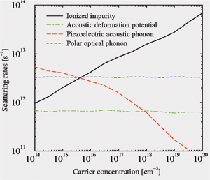
The characterization of the physical properties of strained Si/SiGe and III-V compounds is required for wide ranges of material compositions, temperatures, doping concentrations, etc. Physics-based analytical models for the lattice, thermal, band-structure, and transport properties of various semiconductor materials, as well as models for important high-field and high-doping effects taking place in the devices, are derived and implemented in the device simulator Minimos-NT.

The module on advanced transport models for nanoscale devices is currently focused on III-V nanowire-based devices, where the carrier evolution is dominated by quantum effects. A Wigner transport model has been derived which, along with spatial quantum effects, accounts for quantum dissipative processes due to phonons. A model-based Monte Carlo simulator has been developed and applied by utilizing GRID technologies to investigate the transport process.


Interplay of carrier scattering mechanisms in wurtzite GaN


Home | Activities | Staff | Publications | Sponsors |Contact Us