|
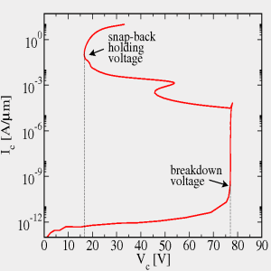
In integrated circuits, interfering signals can drive bipolar configurations into snap-back. This effect is commonly utilized for electrostatic discharge (ESD) protection on input and output interfaces of semiconductor devices. Snap-Back can also happen uncontrolled in parasitic n-p-n structures, and high current densities may cause damage in the structure. Due to the increasing integration density of devices and especially due to the integration of several functional blocks with different power domains on a single chip, snap-back issues have become critical. One important application field is in automotive systems, where smart power devices including power and signal blocks are incorporated and are often exposed to high energetic interfering signals on both supply and data lines. When the breakdown voltage is exceeded and the snap-back state is reached, the current density remains high as long as the applied voltage stays above the snap-back holding voltage. Therefore the destruction process will go on and will cause damage to the device. To avoid this self-destruction process, the goal in designing integrated circuits is therefore to keep this snap-back holding voltage of parasitic bipolar configurations high, at least above the supply voltage. The breakdown voltage lies in the best case above the highest possible voltage that results from interfering signals. Simulation of this snap-back phenomenon allows making design decisions to adapt the structure to increase overall reliability. Simulation allows the investigation of the consequences of changing doping profiles, the shape of the p- or n-wells, or the distances between well borders and contacts. This allows the adjustment of the snap-back holding voltage and the breakdown voltage itself, and dynamic and thermal aspects can be involved in the design. Considering these results in the design of future smart power devices helps to improve the overall reliability.
|