|
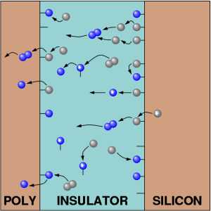
Hydrogen is linked to a number of important phenomena occuring in semiconductor devices. The most important is probably the passivation of undesired electrically active interface defects through hydrogen exposure during processing. During long term operation the interface defects can be depassivated again, leading to a considerable change of the electrical characteristics over time and to increased failure rates. Depassivation can occur, for instance, due to the exposure to higher temperatures, higher gate voltages, and hot carrier injection from the channel in MOS devices. In addition, exposure to highly reactive atomic and protonic hydrogen can result in depassivation as well, depending on a complex interplay of various reactions. In the semiconductor bulk, hydrogen can passivate electrically active shallow dopands, which can also have a profound influence on the electrical behavior of the semiconductor device. As with interface states, these hydrogen/dopand complexes can be broken, again resulting in a shift of the device characteristics. Inside insulators, hydrogen species can interact with or even create new defects, which changes the threshold voltage of MOS transistors. Hydrogen is known to occur in a number of different configurations, most notably as a proton or in molecular form. Atomic hydrogen is known to be unstable but may be an important temporary quantity before it passivates/depassivates a defect or dimerizes into molecular hydrogen. As a consequence, there are two fundamental modeling issues: creation/annihilation of different hydrogen species and the motion of each species through the various material layers. To properly describe the interaction of the hydrogen species with interface, bulk, and oxide defects, a number of reactions have to be considered. The associated reactions depend strongly on the charge state of the defect, further increasing the complexity of the problem. Transport of the hydrogen species may be strongly influenced by shallow and deep traps, resulting in dispersive behavior. In contrast to conventional diffusion, dispersive transport is characterized by an unusually strong spreading of a particle packet, resulting in an extremely long transient tail.
|