|
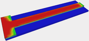
Thin film deposition is a widely used technique for the fabrication of MEMS (Micro-Electro-Mechanical Systems) devices. This technique is required to manufacture free-standing structures which can induce or sense a mechanical movement. During the deposition of new thin layers, an intrinsic stress is generated. After removal of the underlying layer, the deposited layer, which is an important component of the MEMS device, is left free-standing. As a consequence, the process-induced stress can relax and deform the deposited layer in an undesirable and uncontrolled way. In the first phase of the deposition process, islands with varying crystal orientation are formed and grow isotropically. In the course of further deposition, these islands start to coalescence, which forces the islands to grow in height instead of in a direction parallel to the substrate surface. The islands are consequentially transformed from an island shape to a grain-like shape. Another aspect is that the deposition takes place at elevated temperatures. When the temperature decreases to room temperature, the volumes of the grains decrease and the stresses at the grain boundaries increase. The main sources of intrinsic stresses are: coalescence of the grain boundaries, misfit stresses, rearrangement of the atoms, grain growth, and annihilation of excess vacancies. The investigation of stress effects in thin films is focused on the deposition of SiGe on sacrificial layers for cantilever fabrication. The goal of this work is the integration of microstructure models which describe strain development due to grain dynamics in a macroscopic mechanical formulation. This strain loads the mechanical problem which provides a distribution of the mechanical stress and enables the calculation of displacements in the MEMS structure. As a practically fabricated example, a 10 um thick SiGe film was deposited on an oxide sacrificial layer. The deposited thin film with the intrinsic stress is presented in Figure 1a). After removing the sacrificial layer, the 1 mm long cantilever is released (see Figure 1b) and the stress can relax by deflection of the free-standing cantilever. Therefore the high stress areas are reduced.
|