|
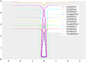
During passivation processes which cover IC (integrated circuit) chips, cracking effects can happen that lead to subsequent device failures. To avoid these effects, which depend on three-dimensional void characteristics versus geometrical parameters of a deposition process structure, a set of three-dimensional investigations has been performed by using our general purpose topography simulator ELSA (Enhanced Level Set Applications). Technologies for image sensor processing are sensitive to passivation planarization, which serves to prevent clear layer coating issues and to shorten the optical path between color filter and sensor surface. A typical passivation process in IC chips uses a layer of silicon dioxide from PECVD (Plasma Enhanced Chemical Vapor Deposition) in a TEOS (Tetraethoxysilane) process covered by a layer of silicon nitride. Therefore, two-dimensional investigations have been performed to achieve planarized passivation of the moisture barrier and the topmost metal layer. A good means to determine whether a passivation layer is planarized or not is the planarization margin. The planarization margin is defined as the distance between the top of the void or the bottom of the oxide dimple (when no void forms) to a line with the specific distance to the flat surface of a trench. Using ELSA the trench width and height have been optimized to guarantee a sufficient planarization margin larger than CMP (Chemical Mechanical Planarization). Figure 1 shows a typical example of our investigations, where D, H, and T stand for trench width, trench height, and the thickness of the passivation layer in um.
|