|
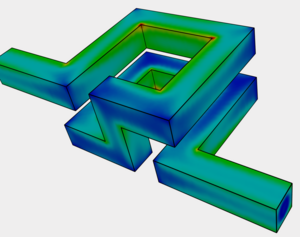
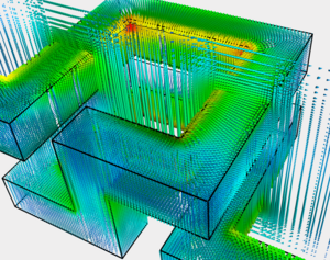
The three-dimensional interconnect structure in integrated circuits represents a difficult electromagnetic system. It includes up to seven metalization layers with links for more than one million transistors hosted on a silicon substrate. A series of physical effects are responsible for the limitation of the maximum allowed frequency of modern integrated circuits. Capacitive and inductive coupling give on-chip noise. Resistance, capacitance, and inductance of the interconnect lines cause rise, fall, and delay times. The skin effect forces the current to pass through the surface of the conductors. An overdriven inductive net produces harmful underdamped ringing step response. Power supply integrity is determined by the on-chip ground and power lines inductance combined with the decoupling capacitance. These effects result in functional failure and depend on the spatial distribution of the interconnect lines. These parasitics must be considered in integrated circuit technology during the design process at an early stage. For this reason, highly accurate models and analysis methods are required to predict and optimize the behavior of interconnect lines for a given layout geometry. These challenging tasks can be significantly supported by three-dimensional interconnect simulation.
The three-dimensional finite element method for the computation of partial differential equations derived from the Maxwell equations is used for the numerical electrical and magnetic field calculation. For the interconnect capacitance and resistance extraction, the electric field is calculated by the Poisson equation. The inductance extraction is based on the magnetic field calculation. The dimension of the interconnects in the integrated circuits allows the assumption of dominant magnetic fields. Thus the magnetic field is calculated by the diffusion equation, which is solved using edge finite element methods. These approaches allow inductance, capacitance, and resistance extraction in complex interconnect structures. Analytical electrical and magnetic field evaluation is used to revise the results of the numerical solution.
|