|
Negative bias temperature instability (NBTI) has come to the forefront of not only academic but also industrial interest. It occurs in p-type MOS devices stressed with negative gate bias at elevated temperatures. In particular for thicker oxides, as used in high-voltage devices, the degradation can be ascribed to two major effects, the generation of interface traps Nit at the Si/SiO2 interface and the generation of fixed oxide charges in the dielectric. These effects lead to a shift of important transistor parameters, such as the threshold voltage Vth, the drain current ID, the transconductance gm, and the off current Ioff. The degradation can cause timing shifts of logic circuits and thus lead to circuit failure. Due to the need for accurate prediction of device and circuit lifetimes, modeling and simulation of the degradation physics has gained in importance.
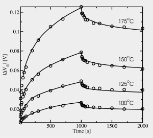
There are two important factors for accurate modeling: (a) the physics of the degradation mechanisms have to be modeled as precisely as possible and (b) the experimental and measurement setup must lead to an exact description of the device state. Here, particularly the applied measurement technique needs special attention, as the method used for evaluating NBTI degradation can have a considerable impact on life-time extrapolation results. The device simulator MINIMOS-NT is used for the simulation of NBTI using an enhanced version of the reaction-diffusion model. The figure shows very good agreement of the implemented model with measurement data for a wide range of temperatures.
|