|
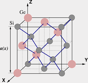
Non-silicon semiconductor materials have become more and more important in the development and implementation of advanced technology nodes. The most prominent of these materials are silicon-germanium compounds, because they facilitate performance tuning via stress engineering, and they are reasonably compatible with silicon-based technology. Therefore accurate simulation modules which can deal with these silicon-germanium compound materials are necessary. One of the most critical process modules is ion implantation, which requires, on the one hand, accurate implantation tables for the analytical simulation analysis of ion implantation and, on the other hand, advanced and well-calibrated Monte-Carlo ion implantation simulation capabilities. Therefore a Monte-Carlo ion implantation simulation module for the accurate simulation of ion implantation into silicon-germanium compound semiconductor material has been developed. Since quantitatively predictive capabilities are a must for a Monte-Carlo ion implantation simulator, extensive evaluation and calibration of the simulation tool on the basis of experimental results is inevitable. For this purpose, a set of specifically selected experiments has been developed and carried out. On the basis of these experiments the independent analysis of the various effects, which characterize the implantation behavior (channeling, damage accumulation) has been feasible. The experimental set-up is clearly distinguishable from usual industrial experimental analysis, which mainly focuses on typical fabrication conditions. Nevertheless, in order to ensure the applicability of the calibration to semiconductor technology requirements, usual silicon wafers with epitaxially grown silicon-germanium layers with various, but typical, germanium contents were used for the experiments. But not only the influence of the compound composition, but also the influence of epitaxially induced stress on the ion implantation behavior was investigated. As a side effect of such a comprehensive experimental analysis, implantation tables for analytical ion implantation simulation modules can also be worked out.
|