


Process Simulation and Virtual Fab
Process TCAD
Process TCAD (Technology Computer-Aided Design) refers to the simulation of fabrication steps in semiconductor manufacturing. As device dimensions continue to shrink and new materials are introduced, experimental process development becomes increasingly costly and time-consuming. TCAD tools address this challenge by enabling predictive modeling of key fabrication steps, such as lithography, etching, deposition, implantation, and annealing.
By capturing the complex interplay of physical and chemical processes at the feature scale, Process TCAD helps engineers design, analyze, and optimize semiconductor processes, reducing cleanroom iterations, improving yield, and accelerating innovation.
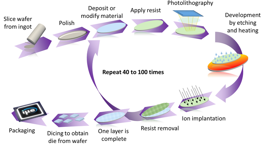
These fabrication steps are not performed just once. Instead, they are repeated across dozens of cycles to construct a complete integrated circuit (IC), with photolithography playing a central role in each iteration (Fig. 1). Our research focuses on simulating this multi-step process in detail, using advanced frameworks and high-performance algorithms. Some of our recent developments and contributions are highlighted below.
ViennaPS Process Simulation Framework
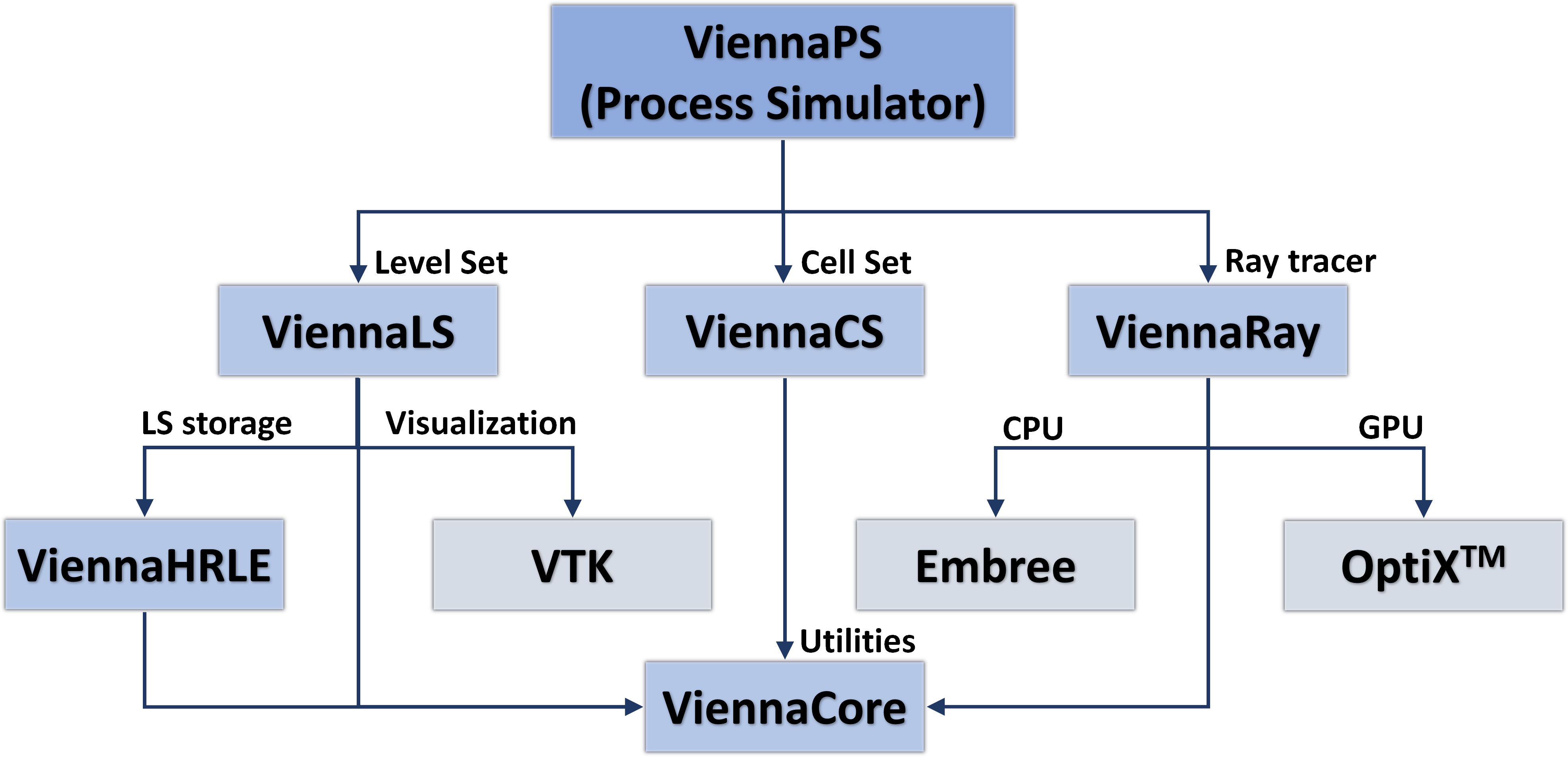
ViennaPS is our open-source, high-performance simulation platform for 2D and 3D feature-scale process modeling. At its core, ViennaPS employs advanced level-set methods to accurately capture evolving material interfaces, while leveraging Monte Carlo ray tracing for simulating the transport and interaction of particles involved in deposition, etching, and other surface reactions.
The framework is highly modular and extensible, providing C++ and Python interfaces that enable customized simulation pipelines and tight integration with data-driven or AI-based workflows. ViennaPS supports a wide range of physical models, including:
• Directional and isotropic etching and deposition
• Sticking, scattering, and re-emission of particles
• Boolean operations and morphological filters
• Complex topographies via mesh-based surface descriptions
A schematic overview of the ViennaPS architecture, showing its integration with level-set solvers, ray tracing backends, and chemical modeling modules, is shown in Fig. 2.
One of the key strengths of ViennaPS lies in its high-performance computing support. Simulations can be accelerated using multi-threaded CPU backends as well as GPU hardware via NVIDIA OptiX™, enabling large-scale or high-resolution models to be executed efficiently. This makes it ideal for applications such as high-aspect ratio etching, gap fill studies, or topography-aware process optimization.
Multi-Scale Process TCAD
Accurate and predictive process simulation requires the integration of multiple physical models spanning a wide range of spatial and temporal scales, from atomistic reactions at surfaces to plasma behavior in the entire chamber. Our multi-scale approach, illustrated in Fig. 3, combines atomistic, feature-scale, and equipment-scale models to achieve physically consistent and computationally efficient simulations for advanced semiconductor processes.
At the atomic scale, techniques such as Density Functional Theory (DFT) and Molecular Dynamics (MD) are employed to compute fundamental material interactions. These models provide critical data, including sputtering yields, adsorption energies, sticking coefficients, and surface passivation dynamics. Such data serve as input parameters for feature-scale simulations, particularly in precision processes like atomic layer etching (ALE) or selective deposition.
At the feature scale, the core of our simulation infrastructure is ViennaPS, a high-performance, open-source simulator based on level-set methods and Monte Carlo ray tracing. It captures the evolution of 2D and 3D geometries under directional fluxes, incorporating physical models for re-emission, shadowing, etching/deposition dynamics, and Boolean operations. ViennaPS supports both CPU and GPU backends, leveraging NVIDIA OptiX™ for ray tracing acceleration, enabling fast, scalable modeling of complex nanoscale topographies such as trenches, vias, and fins.
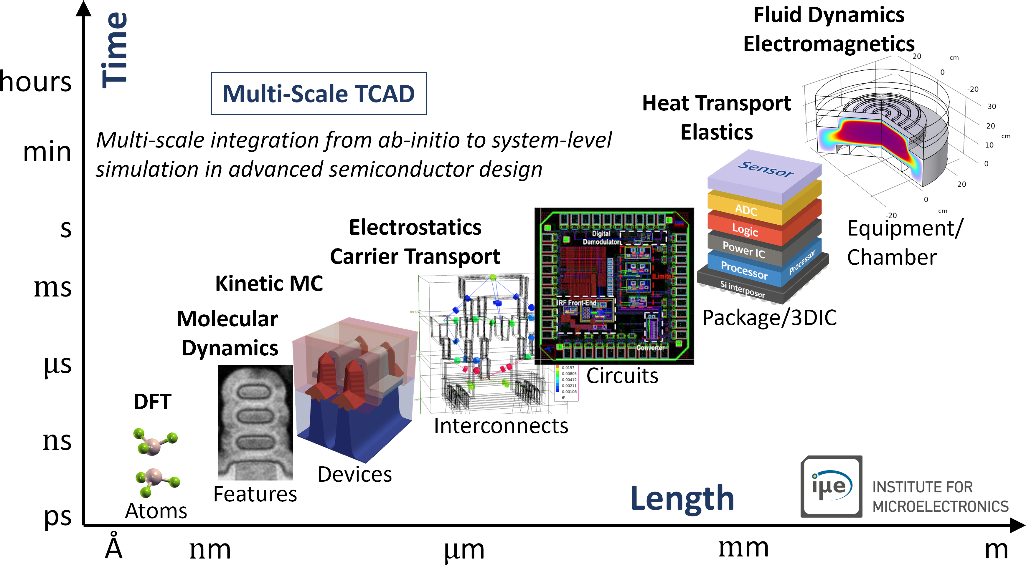
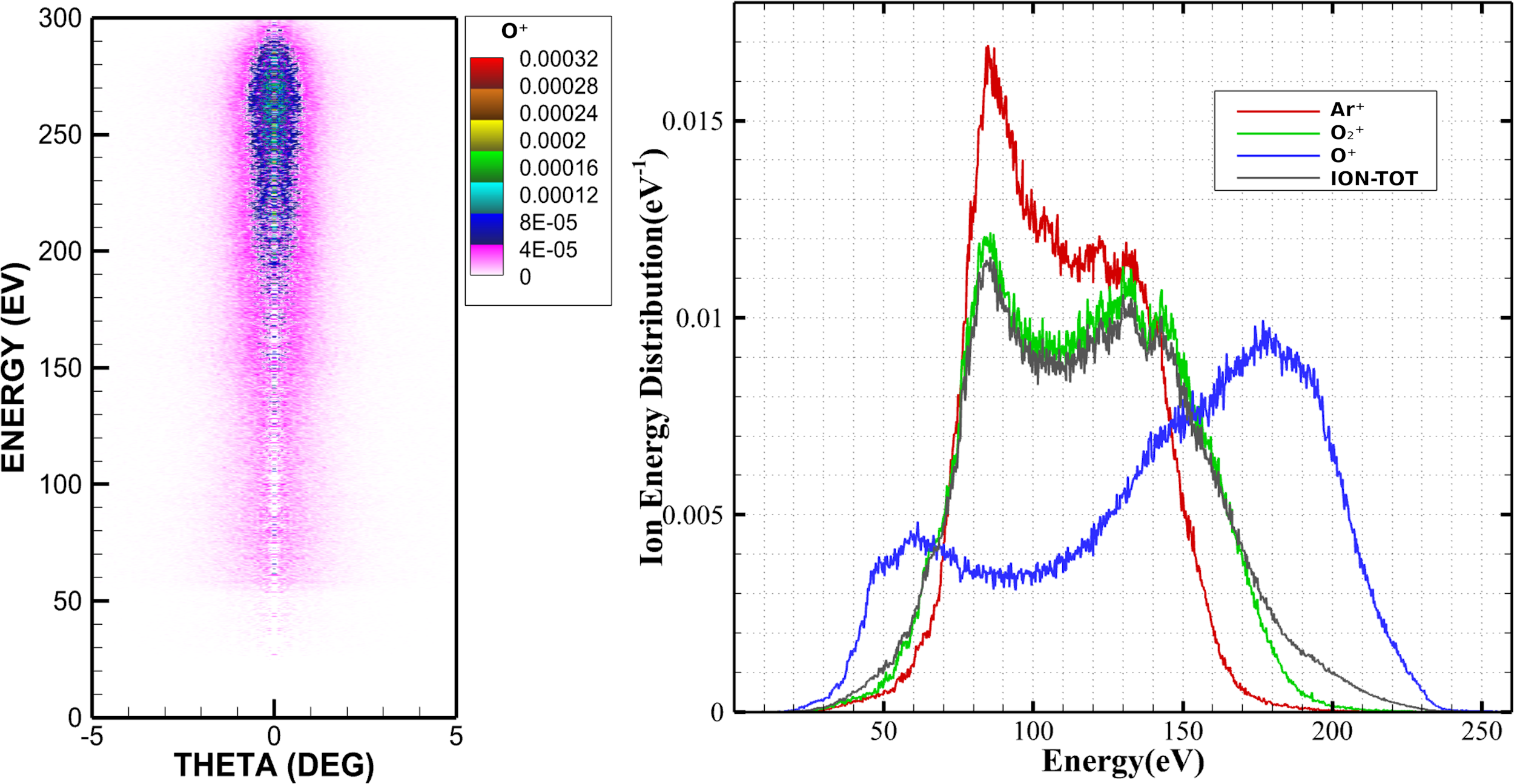
At the equipment/chamber scale, we utilize hybrid models like the Hybrid Plasma Equipment Model (HPEM) to simulate the full reactor environment. These models combine fluid dynamics for bulk plasma transport with kinetic and sheath models that resolve local interactions at the wafer surface. They predict spatially resolved ion and neutral fluxes, along with their energy and angular distributions (IEADs). An example of such a result is shown in Fig. 4, where the ion energy distribution and directionality of different species (e.g., O+, Ar+) are derived from HPEM simulations. These outputs are then interpolated and injected as boundary conditions into ViennaPS, ensuring accurate surface response to realistic plasma environments.
By integrating chamber-level plasma dynamics with feature-scale geometry evolution and atomistic surface physics, this end-to-end modeling framework enables predictive simulation of fabrication steps under real-world conditions. It supports process optimization, equipment design, and design-space exploration, all while reducing experimental cost and iteration cycles. This strategy also sets the stage for advanced capabilities like automated calibration, inverse design, and AI-assisted sensitivity analysis, discussed in section AI for Microelectronics.
Automated Model Calibration and Sensitivity Analysis
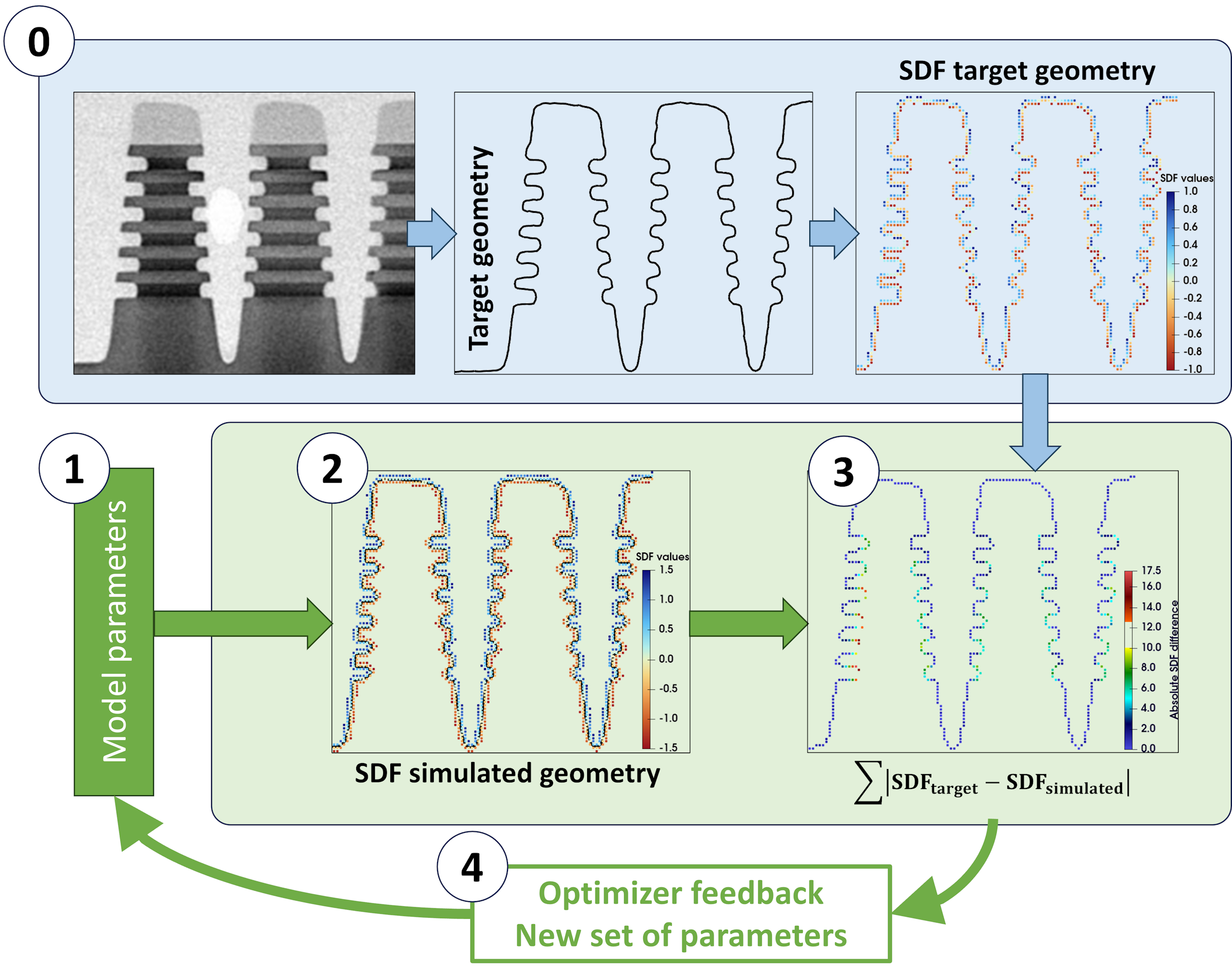
Accurate and predictive process simulation relies on well-calibrated models that reflect experimental reality across a range of operating conditions. To streamline this calibration, we present ViennaFit, an open-source optimization framework tightly integrated with ViennaPS. ViennaFit automates the parameter fitting process by comparing simulated surface profiles with experimental data, such as 2D SEM or TEM micrographs, using advanced discrepancy metrics including area difference (AD) and narrow-band distance (NBD). These metrics quantify geometric mismatches and drive gradient-free optimizers (e.g., dlib, Nevergrad) to iteratively minimize them. Fig.5 illustrates the automated calibration loop in ViennaFit, where signed-distance fields (SDFs) of experimental and simulated structures are compared, and the discrepancy is minimized through optimizer feedback.
Beyond calibration, ViennaFit supports global sensitivity analysis (GSA) using Sobol indices, allowing users to systematically identify which input parameters most strongly affect simulation outputs. This dual capability enables not only efficient calibration but also robust model reduction, design-space exploration, and inverse process design.
Building on this foundation, our research increasingly incorporates artificial intelligence (AI) to further enhance simulation workflows. In particular, machine learning (ML) models trained on hybrid datasets, combining physics-based simulation data with sparse experimental measurements, enable both rapid prediction and greater interpretability. For example, in processes like plasma-enhanced chemical vapor deposition (PECVD), explainable AI techniques such as SHAP have been used to analyze the relative importance and interdependence of key process parameters.
AI methods are also being leveraged for surrogate modeling of complex equipment behavior at the feature scale, accelerating multi-scale simulations and enabling real-time optimization of process conditions. These developments reflect a broader trend toward data-driven TCAD, and are discussed further in the section AI for Microelectronics, where we explore how ML and physical modeling are merged for physics-based and accelerated semiconductor process simulation.
Doping, Implantation, and Annealing
Accurate modeling of doping processes is essential for simulating modern semiconductor devices, where precise control over impurity profiles and defect dynamics directly influences electrical performance. Ion implantation is the industry-standard technique for introducing dopants, offering high precision and scalability. However, it also generates complex damage in the crystal lattice, including vacancies, interstitials, and dopant-defect complexes. These must be carefully annealed to activate dopants while minimizing undesirable defect formation.
Our simulation framework supports ion implantation modeling via 3D dopant deposition profiles, informed by either Binary Collision Approximation (BCA), Monte Carlo (MC) simulations, or experimental inputs. The subsequent annealing phase, crucial for dopant activation and defect healing, is captured using continuum diffusion and clustering models, or increasingly, through atomistic simulations that resolve dynamic defect interactions at the nanoscale.
To better understand these atomic-scale phenomena, we leverage Molecular Dynamics (MD) and Density Functional Theory (DFT) simulations, which provide insight into defect formation energies, migration barriers, and dopant clustering behavior. These simulations reveal how process conditions influence dopant activation and defect stability, especially important for materials like GaN, where p-type doping with Mg remains a major challenge due to defect compensation and segregation during annealing.
We have recently developed several machine-learned interatomic potentials (ML-IAPs) for the Si-C-Al and Ga-N-Mg systems, trained using DFT-calculated data. The potential accurately reproduces defect formation energies and diffusion barriers, enabling large-scale simulations of defect behavior during post-implantation anneals. Such potentials bridge the gap between quantum accuracy and classical MD scalability, allowing realistic modeling of doped semiconductors under processing conditions.
These ML-IAPs represent a critical enabler for predictive doping simulation and will play an increasingly important role in next-generation process TCAD. Their development and integration are further discussed in the section AI for Microelectronics, which outlines how data-driven models are enhancing physical accuracy and computational efficiency across scales.