Semiconductor- and 2D-Based Sensors
While aggressive transistor scaling has been at the forefront of developments in the semiconductor industry for decades, there is currently an increasing demand for added functionalities on a single device, a trend often referred to as "More-than-Moore" integration. This is most evident in the rapid development of integrated smart sensors for industries including smart homes, automotive, and healthcare, alongside the rise of wireless sensor networks and the Internet of Things (IoT). Our research encompasses a broad variety of materials and devices for various environmental and biological sensors, with a specialized focus on engineering two-dimensional (2D) materials at the atomic level to create next-generation sensing platforms.
A major challenge for gas sensors is achieving high selectivity and sensitivity at or near room temperature, which is crucial for low-power applications. While semiconductor metal oxide (SMO) sensors have seen commercial success, their reliance on high-temperature operation complicates integration with standard CMOS technology. Two-dimensional (2D) materials, such as molybdenum disulfide (MoS2), phosphorene, and antimonene, offer a compelling alternative, as their atomically thin structures are extremely sensitive to surface interactions, enabling potent sensing capabilities.
Our research moves beyond conventional approaches by focusing on how the fundamental electrical properties of these materials can be precisely controlled and even exploited. While phenomena like hysteresis are often viewed as a challenge for digital transistors, we are pioneering methods to harness them as a novel mechanism for highly selective gas sensing. We achieve this through an integrated research strategy that combines material synthesis and modification, advanced atomic-scale characterization, and multi-scale computational modeling.
Substitutional Doping and Defect Engineering
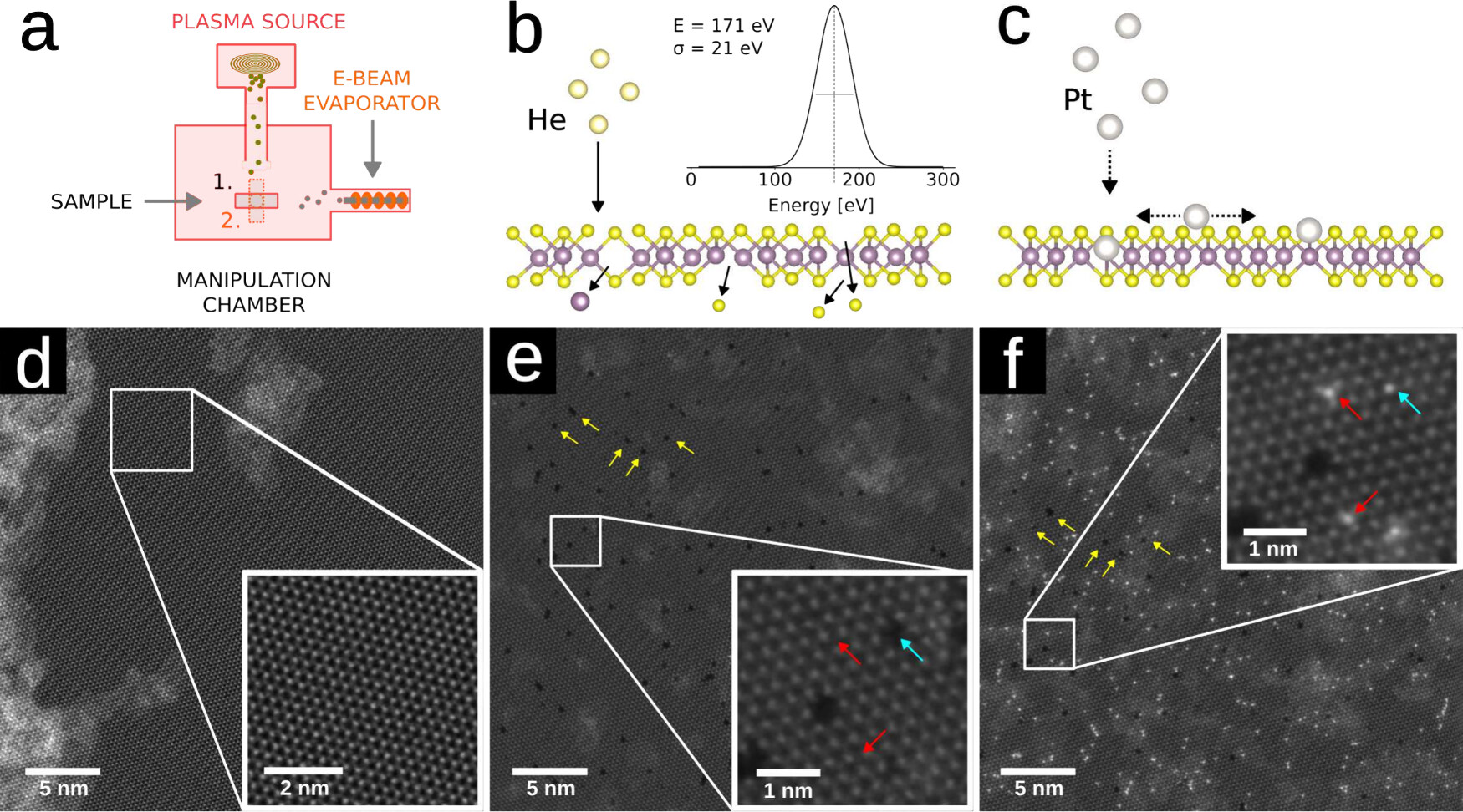
At the core of our research is the ability to precisely modify the properties of 2D materials through substitutional doping. In collaboration with the Physics of Nanostructured Materials group at the University of Vienna, we employ a sophisticated two-step implantation method to introduce specific metal atoms (such as Pt, Au, Pd, Ag, and Ni) into the lattice of materials like MoS2. This technique first uses low-energy ion irradiation (for example, with He+ ions) to create vacancies in the 2D material, followed by metal evaporation in an ultra-high vacuum (UHV) environment to fill these sites. This level of atomic control allows us to engineer the material's surface to have a strong, selective affinity for specific gas molecules like H2, NO2, and NH3. The two-step implantation process is illustrated in Fig. 1.
Harnessing Hysteresis for Selective Gas Sensing
Hysteresis in the electrical characteristics of a field-effect transistor (FET) is typically caused by charge carriers getting trapped at defect sites, often at the interface between the semiconductor channel and the gate insulator. While this is a significant reliability concern for digital logic, our work explores how this phenomenon can be engineered for selective gas detection.
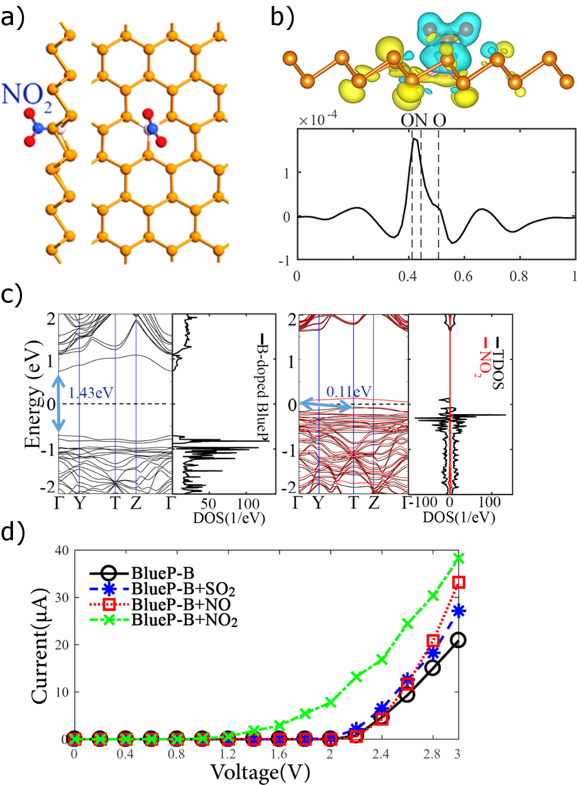
Our central hypothesis is that the adsorption of specific gas molecules on a doped MoS2 surface modulates the charge-trapping dynamics, leading to a unique and identifiable change in the hysteresis loop. This change can arise from two primary mechanisms: the adsorbed molecules may introduce new charge trapping states, or they may cause a shift in the channel's Fermi level, which alters the energetic distance to existing trap states in the material or the gate oxide. The resulting change in the material's electronic structure leads to a measurable change in its electrical response, which forms the basis of the sensing mechanism (Fig. 2).
To investigate these mechanisms, we can perform extensive electrical characterization, including:
- Hysteresis Measurements under various gas ambients (H2, O2, NO2, NH3), pressures, and temperatures to quantify the sensor's response.
- Extended Measure-Stress-Measure (eMSM) Experiments to probe the time-dependent trap dynamics and extract key parameters like trap densities and energy levels.
By systematically studying how different dopants and gas molecules interact to shape the hysteresis, we aim to build a foundational understanding that will allow us to design sensors where the hysteresis profile itself becomes the fingerprint of a specific gas.
Multi-Scale, Physics-Based Modeling
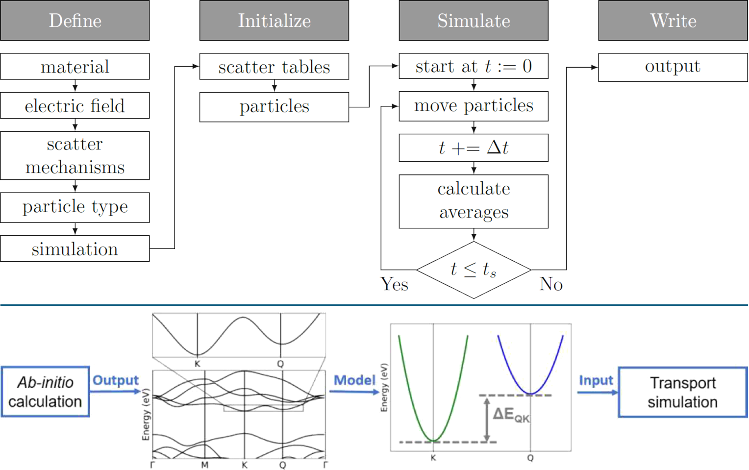
Underpinning the experimental work is a powerful multi-scale modeling approach that connects atomistic material properties to device-level performance. This "materials-to-device" pipeline allows us to predict and interpret experimental results, guiding our efforts in material and device design. Our comprehensive modeling framework, shown in Fig. 3, connects first-principles material calculations to device-level transport simulations.
Ab Initio and DFT Simulations: We use first-principles calculations to investigate the electronic structure of doped and pristine 2D materials. These simulations allow us to calculate gas adsorption energies, predict charge transfer between the surface and a gas molecule, and identify the energy levels of dopant- and adsorbate-induced trap states. We have applied these methods to various materials, including blue phosphorene, antimonene, and MoS2.
Charge Transport Modeling: We utilize our in-house Ensemble Monte Carlo simulator, ViennaEMC, to study phonon-limited electron transport and calculate charge carrier mobilities in these novel materials.
Device-Level Trap Dynamics: The insights from our atomistic simulations and experimental measurements are integrated into our in-house software, Comphy. Using Non-Radiative Multiphonon (NMP) theory, Comphy models the dynamics of charge trapping and release at defect sites. This enables us to simulate the complete hysteresis behavior of a device and predict how it will respond to different dopants and ambient gas conditions, ultimately providing design guidelines for the next generation of 2D material gas sensors.
Through this comprehensive approach, we aim to bridge the gap between fundamental materials science and practical device engineering, paving the way for highly sensitive, selective, and CMOS-integrable sensors for environmental monitoring, medical diagnostics, and industrial safety.
Hot Carrier Solar Cells
Hot carrier solar cells (HCSCs) aim to push photovoltaic efficiency beyond the Shockley-Queisser limit by extracting photogenerated carriers before they thermalize. Achieving this requires slowing carrier cooling and engineering energy-selective contacts. Our research investigates both of these aspects, combining materials modeling and carrier transport simulations to identify and design suitable absorber materials.
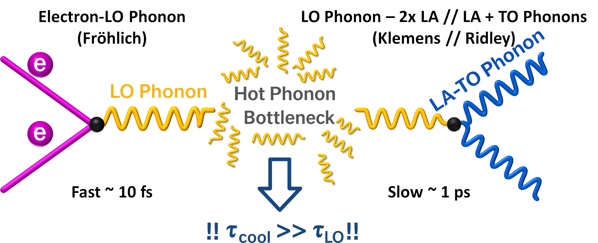
In many materials, carriers rapidly lose excess energy to longitudinal optical (LO) phonons, followed by slower phonon–phonon decay into acoustic modes. This imbalance creates a hot phonon bottleneck (HPB), where reabsorption of LO phonons prolongs carrier lifetimes. This effect, illustrated in Fig. 4, plays a critical role in materials such as lead halide perovskites, where polaron formation and dynamic lattice screening further reduce thermalization rates.
We use ab initio calculations to extract electron-phonon coupling strengths and phonon decay rates, which are fed into Boltzmann transport solvers (ViennaEMC) to model time-resolved carrier dynamics. These insights inform the design of band structures, phonon spectra, and nanostructures that support long-lived hot carriers and facilitate energy-selective extraction.
Integration of Semiconductor Metal Oxide Gas Sensors
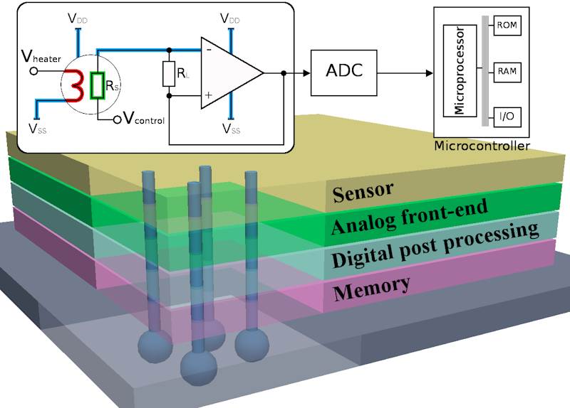
To minimize interconnect length and reduce resistance-capacitance (RC) delay, the ideal integration strategy for gas sensors is direct fabrication within a CMOS process using 3D integration (Fig. 5). This enables compact system-on-chip architectures by embedding the sensor alongside the amplifier, ADC, and microcontroller.
Among solid-state gas sensing technologies, electrochemical, catalytic pellistors, and semiconducting metal oxides (SMOs), SMO sensors stand out for their compatibility with CMOS, low cost, and high sensitivity to a wide range of gases (e.g., VOCs, CO, NH3, H2S).
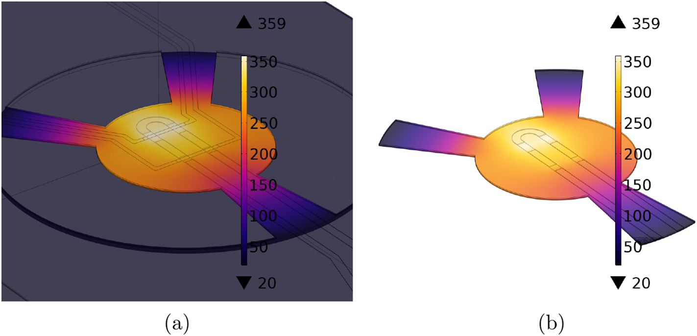
Their key advantages include fast response, scalability, and ease of integration into portable systems. However, SMOs face two key challenges: limited selectivity due to non-specific surface charge modulation, and the need for elevated operating temperatures (250–500 C). To address the latter, we develop microheater arrays capable of generating spatially distinct temperatures across the sensor surface (Fig. 6), using a single power input. This enables tailored surface reactions for improved selectivity and reduces power consumption—supporting applications in wearable and mobile electronics.