|
As the miniaturization of semiconductor devices continues, new challenges such as Negative Bias Temperature Instability (NBTI), Hot Carrier Injection (HCI), and Time-Dependent Dielectric Breakdown (TDDB) are being encountered. Industrial interest is especially focused on NBTI, and a lot of research has already been conducted in this field. However, no convincing model reflecting all relevant mechanisms behind this phenomenon has been developed to date. On the one hand, it appears to be very well established that hydrogen diffusion and reactions play a crucial role in this context. But on the other hand, charging of defects by tunneling is also suspected to constitute a considerable contribution to this phenomenon. Therefore it is worth uncovering the mystery behind tunneling dynamics and incorporating their impact in an extended and more comprehensive NBTI model.
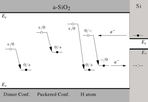
Tunneling is often visualized as a transition of an electron between a state in the silicon conduction band and a "fixed" trap level, irrespective of the charge state of the defect. But in reality, trap levels are subject to a shift due to a relaxation of the defect configuration, a fact that has not been paid very much attention so far and which, however, alters the tunneling dynamics considerably. Two distinct trap levels arise, one for tunneling into and one for tunneling out of a trap, as illustrated in the figure. Only the combination of both levels governs the behavior of a defect. Density Functional Theory (DFT) simulations provide a good opportunity to tackle the calculation of defects energetics. For example, the oxygen vacancy in the puckered configuration is allowed to capture an electron or a hole from the silicon, but it will not appear as a negatively charged defect. The oxygen vacancy in the dimer configuration exhibits a trap level located too far away from the silicon band edge, and therefore this defect will be ruled out for tunneling mechanisms. The hydrogen atom is found not to interact with the interface. Several other defects, including the hydrogen bridge and some atomic-scale models of E' centers motivated by EPR measurements, have also been thoroughly investigated, helping to clarify the picture of the mechanisms underlying NBTI.
|