|
Recent years have seen a continuous shrinking of semiconductor device sizes.
Since operating voltages and currents have not decreased at the same pace,
field strengths, current densities, and power densities are steadily
increasing. Once the electrical and thermal exposure of the semiconductor and
insulator materials involved reaches a critical level, reliability issues
become a major concern for manufacturers and researchers. Currently one of
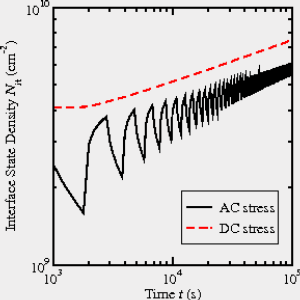
the most intensively discussed reliability issues in CMOS technology is Negative
Bias Thermal Instability (NBTI), the degradation of certain pMOSFET
parameters, foremost the threshold voltage, when the transistor is stressed
with highly negative biases at high temperatures. The underlying
micro-physical effects of NBTI are still unknown, much like the heavily
debated topic of a macroscopic model, which must be able to describe both the
stress phase of the device and, more importantly, the relaxation phase. Such a
model is essential for the analysis of NBTI on a circuit level, since the
artificial NBTI measurement scenario, with determined stress- and consecutive
relaxation phases, is normally not encountered inside electronic circuits.
Instead, the signals at the transistors' gates are stochastic processes,
making reliable simulation models on the circuit level, as well as on the system and
microscopic levels, a necessity. Furthermore, these models are a valuable
aid in investigating new circuit configurations that either minimize the
stress conditions of its transistors or are less susceptible to NBTI. In
the same vein, a sound microscopic model provides clues to how the effects of
NBTI can be reduced in the individual transistors.
|