|
The three-dimensional interconnect structure in integrated
circuits represents a complicated electromagnetic system. It includes
many metalization layers with links for more than one million
transistors and is characterised by resistance, capacitance and
inductance parameters which govern the electric signal behavior
and supply. These parameters usually result in functional failure
and depend on the spatial distribution of the interconnect lines.
It is necessary to investigate the structure of interest during an early stage of the design process,
obtaining its parameters and estimating their impact on the entire
electric circuit.
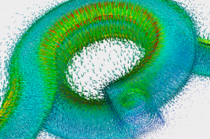
A changing magnetic field influences the electric current
density distribution within an electric conductor. The current
is forced to pass through the surface of the conductors,
which is known as skin effect. If the current is flowing through
several conductors or a wound wire coil, the current density distributes
to minimize the area inside and flows to smaller regions.
This behavior is termed proximity effect. The combination of skin
and proximity effects significantly increases the AC resistance of the
conductor compared to its DC resistance. Thus the skin effect and the
proximity effect must also be taken into account. To extract the
parameters and to consider the skin and proximity effects an
electromagnetic analysis is performed. This is actually a problem of
solving a set of Maxwell equations in the domain of interest with given
boundary conditions. Unfortunately such boundary-value problems can be
solved analytically only for a few special cases. In general, for
arbitrarily shaped domains, numerical approximation methods like the
finite element method (FEM) are used. They give the electric and
magnetic field intensity distribution, the electric potential
distribution, and the electric current density distribution in the
investigated regions, which provide the effects presented above
and are used for the calculation of further parameters. Thereby scalar
and vector shape functions are used.
|