Erasmus Langer
Siegfried Selberherr
Oskar Baumgartner
Hajdin Ceric
Johann Cervenka
Siddhartha Dhar
Robert Entner
Otmar Ertl
Wolfgang Gös
Klaus-Tibor Grasser
Philipp Hehenberger
René Heinzl
Clemens Heitzinger
Andreas Hössinger
Gerhard Karlowatz
Markus Karner
Hans Kosina
Ling Li
Gregor Meller
Goran Milovanovic
Mihail Nedjalkov
Alexandre Nentchev
Roberto Orio
Vassil Palankovski
Mahdi Pourfath
Philipp Schwaha
Viktor Sverdlov
Oliver Triebl
Stephan Enzo Ungersböck
Martin-Thomas Vasicek
Stanislav Vitanov
Martin Wagner
Paul-Jürgen Wagner
Thomas Windbacher
Robert Wittmann

Vassil Palankovski
Dipl.-Ing. Dr.techn.
palankovski(!at)iue.tuwien.ac.at
Biography:
Vassil Palankovski was born in Sofia, Bulgaria, in 1969. He received the diploma degree in electronics from the Technical University of Sofia in 1993. Afterwards he worked for three years in the telecommunications field. In March 1997, he joined the Institute for Microelectronics at the Technische Universtität Wien, where he received the doctoral degree in technical sciences in 2000 and continued as a post-doctoral researcher. In summer 2000 he held a visiting research position at LSI Logic Corporation, Milpitas, California. In 2003 Dr. Palankovski and Dr. Quay published the book Analysis and Simulation of Heterostructure Devices in the Springer series on Computational Microelectronics. In 2004, he joined Infineon Technologies, Villach, Austria, for half a year as technology development engineer. Having received the highest Austrian award for young scientists (START-Preis), Dr. Palankovski returned to the Technische Universität Wien in February 2005 to establish the Advanced Materials and Device Analysis group.

Analysis and Simulation of Advanced Heterostructure Devices

A large project (START) on "Simulation of Advanced Semiconductor Devices", funded by the Austrian Federal Ministry for Science and Research (BMWF) through the Austrian Science Fund (FWF), has entered into its third year with positive international evaluation.
The project includes several research topics, such as modeling of novel semiconductors (strained Si/SiGe, various III-Vs, as well as the Group IV-VI material systems). The device applications include advanced high-frequency high-power heterojunction bipolar transistors (HBTs) and high electron mobility transistors (HEMTs), as well as quantum wires and high-efficiency solar cells.
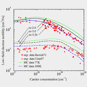
The physical material properties of wide ranges of material compositions, temperatures, doping concentrations, etc. are analyzed using Monte Carlo (MC) simulation. New 2D Ensemble Monte Carlo code was developed and verified versus bulk MC code for different materials. It is used as a platform for the development of 2D Wigner quantum MC code.
Physics-based analytical models for the lattice, thermal, band-structure, and transport properties of various semiconductor materials, as well as models for important high-field and high-doping effects taking place in the devices, are derived and implemented in the device simulator Minimos-NT. The models are calibrated against experimental data from our scientific partners. Novel device structures are investigated, designed, and optimized.


Low-field electron mobility in n-PbTe, as a function of free carrier concentration at 77K (open symbols - experiment, dashed lines - simulation) and300K (filled symbols - experiment, solid lines - simulation). The impact of the non-parabolicity factor (alpha) of the L-valley is demonstrated.


Home | Activities | Staff | Publications | Sponsors |Contact Us