|
Highly integrated microelectronic circuits (e.g., microprocessors) require dense interconnects with dimensions down to some 150 nm. With the resulting increase in current density in the interconnects, electromigration-induced failure becomes a more and more challenging issue. Significant advances have been made by choosing copper instead of aluminum as an interconnect metal, because copper has an improved electromigration bulk resistance.
State-of-the-art copper interconnect technology imposes new challenges for electromigration reliability Technology Computer-Aided Design (TCAD) solutions. One major problem of copper interconnects is high diffusivity at the interfaces to cap and barrier layers. In particular, when new materials and processes are introduced, the adhesion between copper and the attached layers is increased so that the interfacial diffusivity is reduced to the level of the diffusivity of the grain boundaries. This means that the microstructure of the interconnects, i.e., the network of grain boundaries, the crystal orientation inside the grains, and the stress dependence of the grain bulk diffusivity, plays a crucial role in determining the interconnect behavior under the impact of electromigration.
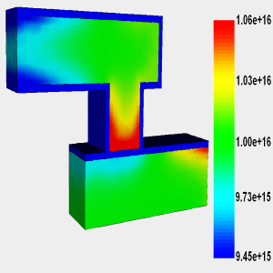
For an efficient electromigration simulation, all driving forces for atom migration should be taken into account. These forces are due to concentration, voltage, temperature and stress gradients. Moreover, the induced stresses cause the anisotropy of the self-diffusion process and should also be considered.
Currently, the electromigration model has been implemented in FEDOS (Finite Element Diffusion and Oxidation Simulator) for three-dimension geometries. All important driving forces have been taken into account in the vacancy transport equation, and the anisotropic material transport generated by the stresses has also been implemented.
|