|
With the advent of strain engineering in CMOS technology, the modeling
of carrier transport in anisotropic media has gained considerably in
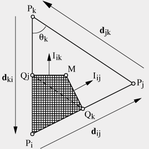
importance. Today's TCAD tools widely employ the Scharfetter-Gummel
(SG) discretization scheme for the convection-diffusion equation. This
scheme is derived assuming current conservation along the edges of a
mesh. However, for certain applications, such as magnetotransport and transport
in anisotropic media, the one-dimensional treatment of the
edge currents is no longer sufficient and two-dimensional extensions
of the SG scheme have to be sought. An established solution to this
problem is the so-called edge-pair method, which attempts to reconstruct a
current density vector for a triangular element from three projections
on the edges, whereby these projections are again determined by the
one-dimensional SG expression. In this project an alternative method
of extending the SG scheme to higher dimensions has been
pursued. Exponential shape functions have been derived from an analytical
solution of the two-dimensional carrier continuity equation. The
shape functions have been defined for triangular elements and vary
exponentially in the direction of the element field vector and
linearly in the direction orthogonal to the element drift velocity
vector. A conservative discretization scheme has been constructed by
means of the box method and implemented in Minimos-NT.
Quantum effects determine transport in emerging nano-electronic
devices. The importance of inter-subband coupling in single- and
double-gate silicon-on-insulator MOSFETs has been
further investigated. It has been demonstrated that
in a double-gate MOSFET, degeneracy effects lead
to a higher occupation of upper subbands due to
a carrier concentration twice as large as in a single-gate structure
for the same gate voltage. This leads to an increase in
inter-subband scattering, which explains the mobility lowering
observed experimentally. Higher substrate occupation of higher
subbands due to degeneracy effects is responsible for the
mobility degradation in ultra-thin body double-gate MOSFETs with (100)
body orientation. A Monte Carlo simulator was used to study the
mobility in MOSFETs under general stress conditions. It has been shown that
the effective mass change due to shear strain results in a substantial
mobility enhancement in the direction of tensile strain. To explore the
physics of carbon nanotube (CNT) FETs and to optimize their
characteristics, self-consistent quantum mechanical simulations based
on the Non-Equilibrium Green's Functions (NEGF) formalism have been
performed. Numerical methods to reduce computational cost and memory
requirements have been developed in order to enable large-scale
applications, such as device optimizations. The effect of
electron-phonon interactions on the device characteristics has been
studied in detail. In agreement with experimental data, our results
indicate that scattering with high energy phonons reduces the
on-current only weakly but can increase the switching time
considerably, due to charge pileup in the channel.
The aim of the next project was the simulation of complete organic
devices based on amorphous semi-conducting hydrocarbons. Attention was
paid both to electric currents in the bulk and to the injection and
extraction of charges at the electrodes. A three-dimensional kinetic
Monte Carlo simulator covering heterojunctions, molecular doping, metal
interfaces, image charge effects at metals, interband transitions, and
arbitrary space charge accumulations has been developed, tested, and
optimized with regard to computational issues. For calibration, the
dark current characteristics of zinc phthalocyanine has been used.
Organic devices most frequently show contact-dominated behavior. So do
the simulations performed. The physics of organo-metallic
heterojunctions is far from being elucidated in detail. Therefore,
the simulations performed focused on the charge dynamics at the
interface, testing various models for the interfacial structure
suggested in the literature, like wave function decays and densities
of states depending on the distance to the contact. The comparison
with the empirical data of zinc phthalocyanine shows, however, that
for this compound, tunneling has to be enhanced significantly in the
simulator, since the latter reproduces thermionic emissive behavior,
analogous to that predicted by the Richardson-Schottky model.
Research on analytical modeling of charge transport and contact
characteristics in organic devices has continued.
A diffusion-controlled injection model has been
developed, assuming drift-diffusion and multiple-trapping transport
theory. This model can explain the dependence of injection current on
temperature, electric field, and the energy barrier between metal and
organic semiconductors. Good agreement between model and experimental
data has been found. Finally, a model describing Space-Charge-Limited
Current (SCLC) has been developed, based on hopping transport and a
Gaussian Density of States (DOS) function. By treating the states at
the center of DOS as transport sites and those in the tail as
trapping sites, the model predicts an essentially quadratic dependence
of the SCLC on voltage.
|