|
In optical transmission systems an operation at 1.3um and 1.55um wavelengths
is preferred, due to the low attenuation in fiber-optic cables. Germanium is an
attractive candidate for high-speed photodetector applications, due to its high
electron mobility and high optical absorption coefficient in this wavelength
range. Recently, a bandwidth of 10GHz has been demonstrated at a wavelength of
1.3um for a PIN-photodiode, fabricated in epitaxial Ge-on-Si technology. The use
of Ge-on-Si technology allows the integration of germanium-based PIN-photodiodes
with CMOS circuits on a silicon chip so that optical communication receivers can be built
with low fabrication costs. However, the accurate simulation of ion implantation
processes, particularly in germanium, is required for the optimization of doping
profiles in optical applications. Boron and arsenic implantations have been studied
in high germanium content SiGe alloys (Ge content >50%) and in pure germanium by
using our Monte Carlo ion implantation simulator MCIMPL-II and SIMS measurements.
We have shown that the calibrated ion implantation simulator can accurately predict
the dopant profiles for different energies and doses. The simulator can estimate
the vacancies and amorphized regions produced in the crystal, which are associated
with a specific implantation profile. We found that the generated point defects
in germanium are significantly reduced compared to silicon, which is consistent
with former experimental observations indicating that boron-implanted germanium
remains essentially crystalline. The simulated point responses revealed that the
boron distribution is significantly reduced in germanium in the vertical direction,
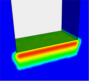
while the lateral profile is quite similar in silicon and germanium. The figure
shows the schematic top and cross-sectional views of interdigitated germanium
PIN-photodiodes as well as the simulated 15keV boron implantation step for the
p+ finger formation in the germanium layer using a photoresist mask.
|