|
The MOS capacitor (MOSCAP), the heart of the
MOSFET, has been addressed by numerical simulations within a
semi-classical treatment for decades. Due to the strong impact of quantum mechanical
effects for MOS inversion layers, quantization effects have been taken into account
assuming two-dimensional sub-band states. For accumulation layers, this is
highly problematic because in addition to the discrete states, there is a nonnegligible
contribution of the continuum states.
A more rigorous investigation carried out by applying the Non-Equilibrium Green's
Functions (NEGF) formalism does not suffer from this problem and directly
yields the current. The influence of level broadening due to the scattering
process was modeled by means of an optical potential.
An analysis of the MOSCAP has been carried out using the NEGF
formalism. The gate and the bulk regions have been assumed to
be in thermal equilibrium, which implies a constant Fermi level. The leakage current
through the gate oxide, which separates the equilibrium regions, has been
calculated assuming ballistic transport between the two reservoirs. The
optical potential, which follows from the carrier lifetime, is added to the
diagonal elements of the Hamiltonian of the reservoirs.
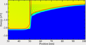
Fig. 1 shows the local density of states of the device under a gate bias of 1.2 V.
The peaks at the resonance energies which correspond to the quasi-bound states
give the main contribution to the gate leakage current.
Although the resonance width is strongly affected by the carrier lifetime, there
is only a slight change in leakage current. It was shown that the macroscopic
quantities are only slightly affected by the optical potential.
|