|
Novel high electron mobility transistors based on III-V materials present the current state of the art in radio frequency power applications. In order to fully develop the potential of the devices, an accurate simulation model is needed. We employ a Monte Carlo technique to investigate stationary electron transport in GaN and InN. We use the simulated data as a basis for the development of analytical models for the simulation of GaN- and InN-based electron devices. We analyze AlGaN/GaN HEMTs featuring various breakdown-enhancement techniques using the two-dimensional device simulator Minimos-NT. Since the longitudinal electric field in the channel reaches peak values of above 500 kV/cm, a hydrodynamic approach is used to properly model the electron transport and energy relaxation. A significant improvement of the device performance has been achieved by adopting the field plate / shield plate techniques. The main goal is to reshape the electric field distribution in the channel and to reduce the peak value on the drain side of the gate edge.
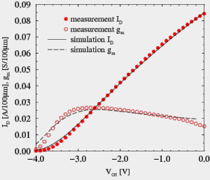
Using two-dimensional device simulations, we optimize the electric field distribution in the channel by varying the geometry of the field plate. Further, we study the AC characteristics of the devices. Exploring different mobility models, we achieve good predictive results for RF transconductance, capacitances, and cut-off frequency for devices with various geometries.
|