Charge Trapping and Variability in CMOS Technologiesat Cryogenic Temperatures
2.2 Bulk Oxide Defects
While in the early days of MOSFETs interface defects have been in the center of research, later also defects in the bulk oxide were added to a more complete description of device degradation.
2.2.1 Oxide Defects in Amorphous SiO2 (a-SiO2 )
Bulk SiO2 is very well understood from both experimental characterization and theoretical studies. One intensively investigated defect candidate for a-SiO2 is the oxygen vacancy (OV) [143, 144,
145]. It forms naturally during oxidation and is essentially a missing O atom in a SiO2 network (where an O atom ideally bonds with two neighbored Si atoms) which leads to a Si-Si bond. The defect is shown in the neutral
(1) and positive (2) charge state in Fig. 2.3, whereby the prime  denotes a metastable configuration which can be accessed via a thermal transition, as explained in Section 3.3. When the
neutral OV traps a hole, the distance between the two Si atoms increases. As a consequence, the Si-Si bond can break, resulting in a Si dangling bond [146].
denotes a metastable configuration which can be accessed via a thermal transition, as explained in Section 3.3. When the
neutral OV traps a hole, the distance between the two Si atoms increases. As a consequence, the Si-Si bond can break, resulting in a Si dangling bond [146].
As shown in Fig. 2.3, the bond breaking and relaxation into a new stable configuration of the oxygen vacancy could be theoretically described by a 4-state
model with the states  , and
, and  . However, various first principle studies show that the energetic position of the defect inside the band structure of the insulator is too far below the valence band or too far above the conduction band of the Si
substrate [147, 148, 149]. Therefore, oxygen vacancies are very unlikely to capture holes and stay neutral in pMOS transistors with relatively thin a-SiO2 oxides and thus do most likely not contribute to BTI or RTN.
. However, various first principle studies show that the energetic position of the defect inside the band structure of the insulator is too far below the valence band or too far above the conduction band of the Si
substrate [147, 148, 149]. Therefore, oxygen vacancies are very unlikely to capture holes and stay neutral in pMOS transistors with relatively thin a-SiO2 oxides and thus do most likely not contribute to BTI or RTN.
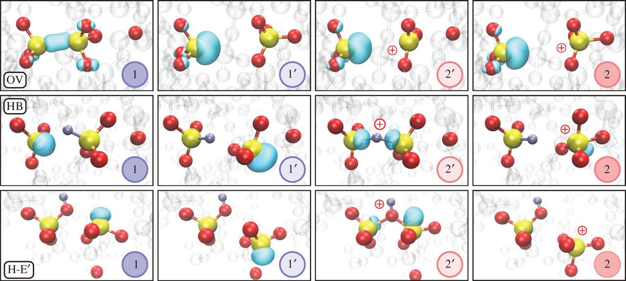
Figure 2.3: The atomistic configurations of the oxygen vacancy (OV), the hydrogen bridge (HB) and the hydroxyl-E’ center (H-E’) show that these defects can be described with a 4-state NMP model. The defects show two
stable configurations  and and can switch between theses stable states via the meta-stable states
  and
and  . The turquoise bubbles show the highest occupied molecular orbital (HOMO) electron distributions. Figure reprinted with permission of the Royal Society from [149].
Recent studies suggested that hydrogen related defects are responsible for reliability degrading phenomena like BTI and RTN [150, 151]. As hydrogen is commonly used in device processing to passivate dangling bonds at the interface between semiconductor and SiO2 , the formation of defects involving H is very likely [151]. In addition, H has the ability to easily diffuse in the SiO2 layer where it can form electrically active defects such as the hydrogen bridge (HB) and the hydroxyl-E’ center (H-E’) [152, 153].
The H atoms diffusing into the SiO2 layer can react with oxygen vacancies, which other ways would stay neutral. When the H atom binds to a Si atom, the resulting defect configuration which involves two Si atoms is called hydrogen bridge (HB). In its neutral configuration, a bond is formed between the H atom and a single Si atom. As can be seen in Fig. 2.3, the Si bonded to the H atom can transit through the triangle spanned by oxygen atoms and the hydrogen atom can then bind to the second Si atom, leaving the first one uncoordinated. By capturing a hole, the HB can form the stable positive configuration 2, which is called puckered. The transition from the unpuckered to the puckered configuration takes place by passing one of the two metastable states 1’ or 2’.
While in the HB configuration the hydrogen atom binds to the silicon atom, it can also have a binding with the oxygen atom and form a hydroxyl-E center (H-E center). These defects can only occur in a-SiO2 , because they need strained Si-O bonds to get formed. The hydrogen atom can break such a strained bond and bind to the oxygen, forming a hydroxyl group (OH). The
same puckering configuration which occurred in the OV and the HB can also occur for the H-E’ center and the trap dynamics can be approximated with a 4-state model.
While OV have trap levels far below the valence band or far above the conduction band of Si, hydrogen related defects show trap levels close close to the Si band edges, as can be seen in Fig. 2.4. Therefore, they are much more important in terms of understanding the mechanisms behind RTN and BTI.

Figure 2.4: The trap levels of various studied defect candidates in HfO2 , SiO2 and SiON are spread across the band gap of all host materials. The trap levels of oxygen vacancies (OV) are far away from the Si conduction
band and therefore play a minor role in BTI and RTN. The trap levels of hydrogen related defects, as the hydroxyl-E center or the hydrogen bridge, and interface defects, as the Pb center or the KN center are on the other hand close to the Si band edges, which makes them highly relevant in terms of BTI. In addition, intrinsic
charge trapping caused by polarons is responsible for electron trapping in high-κ devices.
While most defect studies focus on charge trapping caused by defects, the explanation of some experimental studies require trap bands which can not directly be linked to any known defect candidates [154, 155]. This type of charge trapping can play a major role in wide bandgap devices as SiC. It can happen spontaneously in a-SiO2 and is caused by structures with elongated Si-O bonds, which allow the localization of an additional electron at a certain Si atom [156]. Their trap band lies close to the Si conduction band edge as can be seen in Fig. 2.4.
2.2.2 Oxide Defects in SiON
Plasma-nitrided oxides (PNO) are routinely employed in Si technology to decrease the gate leakage current [157]. However, this comes at the price of a high concentration of nitrogen atoms at the oxide-semiconductor
interface. For these oxides, KN centers become the dominating defect configuration instead of Pb centers [158, 159, 160]. KN centers occur in silicon nitride Si N
N and form during nitration. The central Si atom is back-bonded to an N atom and forms a dangling bond, in which the dangling Si atom is connected to three neighboring N atoms [161, 162]. SDR and SDT magnetic
resonance measurements show that KN centers are located in the vicinity of the interface region of PNO devices and suppress Pb centers. Thus, while in SiO2 devices Pb centers are central for the NBTI
behavior, NBTI is dominated by KN centers in PNO devices [157]. While the defect candidates of near interface defects changes, hydrogen related defects can still play a major role in nitrided oxides, because H atoms
are used for passivating Pb centers [113, 163]. In contrast to Pb centers, which follow a broad energy distribution with at least two peaks, one directly above and one directly below midgap, KN centers are
very narrowly distributed and the distribution of their energetic trap level is very close to the Si-midgap, see Fig. 2.4 [157].
and form during nitration. The central Si atom is back-bonded to an N atom and forms a dangling bond, in which the dangling Si atom is connected to three neighboring N atoms [161, 162]. SDR and SDT magnetic
resonance measurements show that KN centers are located in the vicinity of the interface region of PNO devices and suppress Pb centers. Thus, while in SiO2 devices Pb centers are central for the NBTI
behavior, NBTI is dominated by KN centers in PNO devices [157]. While the defect candidates of near interface defects changes, hydrogen related defects can still play a major role in nitrided oxides, because H atoms
are used for passivating Pb centers [113, 163]. In contrast to Pb centers, which follow a broad energy distribution with at least two peaks, one directly above and one directly below midgap, KN centers are
very narrowly distributed and the distribution of their energetic trap level is very close to the Si-midgap, see Fig. 2.4 [157].
2.2.3 Oxide Defects in HfO2
The continuous miniaturization of MOSFETs has lead to a constant scaling of the insulator thickness to increase the gate capacitance and thus the drive current. However, with decreasing insulator thickness, leakage currents
increase, which leads to several problems, such as higher steady state power consumption which in turn results in heat dissipation and a reduced device reliability. Therefore, the development of alternative insulators with
comparably large dielectric constants (SiO2 :  ), such as the so-called high-κ materials HfO2 (
 ), ZrO
 () or AlO (
 ) became necessary to increase the gate capacitance without introducing leakage effects.

Compared to SiO2 , HfO2 shows a higher degree of disorder as can be seen in Fig. 2.5. Thus, intrinsic charge trapping is suspected to be a central reliability issue in HfO2 based oxides [165]. Contrary to SiO2 , HfO2 is a non-glass forming oxide, which means that it has varying coorination numbers depending on the oxide phase. Furthermore, it is known that HfO2 can (partially) crystallize during annealing which introduces additional structural uncertainties [166]. This opens possibilities for various defect candidates and makes modeling of HfO2 insulators extremely challenging. It is proposed that HfO2 can form electron polarons, which can be stable at room temperature and could be responsible for PBTI. The formation is driven by uncoordinated Hf-ions which can trap electrons. A trapped electron can localize at multiple Hf sites, enabling the formation of a ring where the Hf atoms are pulled towards the center while the O anions are pushed outwards [165, 167].
Some of the defect types discovered in a-SiO2 can also be found in a-HfO2 . For example, the OV occurs in HfO2 , where it is known to form neutral, positive and negative states [168]. It is assumed that the negative states could be responsible for the high density of electron traps observed in high-κ-devices [136, 169]. Various works show trap levels of 1.2 eV to 1.8 eV below the conduction band of HfO2 which have been associated with oxygen vacancies [169, 170]. However, recent first principle studies suggest that the energy level of oxygen vacancies lies closely below the conduction band of HfO2 . According to these calculations, the defect bands measured in [136, 169, 170] can not be linked to oxygen vacancies.
As has been discussed, several trap candidates have been identified that affect the high-perfomant operation of MOSFETs. These defects can exists in various configurations which exhibit different properties. In order to describe the defects and make their impact accessible to device simulators, various models have been discussed in literature which will be presented in the following chapter.