Charge Trapping and Variability in CMOS Technologiesat Cryogenic Temperatures
8.2 Temperature Dependence of BTI Measurements
BTI characterization has been performed by applying the eMSM scheme on Tech. A and Tech. B for a range of temperatures and stress voltages. Following measurement parameters have been used:
-
• Tech. A: For
 BTI measurements have been conducted on
  devices using a stress voltage of
 ![\( \vg [,s]=\SI {2}{\volt } \)](draftv0-images/1D1422837FC29251E4AC309140809569.svg) for nMOS and
for nMOS and ![\( \vg [,s]=\SI {-2}{\volt } \)](draftv0-images/B73575E9589A8FFA3F863A860277D830.svg) for pMOS devices. Phase 2 and phase 3 in the eMSM measurement scheme have been repeated 5 times using the following stress and recovery times:
for pMOS devices. Phase 2 and phase 3 in the eMSM measurement scheme have been repeated 5 times using the following stress and recovery times: ![\( (\ts ,\tr )\in [(\SI {10}{\micro \second },\SI {10}{\second }), (\SI {1}{\milli \second },\SI {100}{\second }), (\SI {100}{\milli \second },\SI {100}{\second }), (\SI {10}{\second
},\SI {1}{\kilo \second }), (\SI {1}{\kilo \second },\SI {10}{\kilo \second })] \)](draftv0-images/332A3B714B99DE3B86840FD925B64269.svg) .
.
-
• Tech. B: For
 BTI measurements have been conducted on
  devices using a stress voltage of
 ![\( \vg [,s]\in (\pm \SI {4.51}{\volt },\pm \SI {5.1}{\volt }) \)](draftv0-images/6D4B0452A91171BC6742E25A7099FCDC.svg) where the positive sign refers to measurements on nMOS and the negative sign to measurements on pMOS devices. Phase 2 and phase 3 in the eMSM measurement scheme have been repeated 5 times using following
stress and recovery times: .
where the positive sign refers to measurements on nMOS and the negative sign to measurements on pMOS devices. Phase 2 and phase 3 in the eMSM measurement scheme have been repeated 5 times using following
stress and recovery times: .
The extracted recovery curves for the measurements of Tech. B are shown in Fig. 8.3 and have been published in [MJC4]. At room temperature, immediately after stress a  shift of about ±100 mV has been measured for the longest stress time, where the positive sign refers to PBTI on nMOS and the negative sign to NBTI on pMOS. Towards cryogenic temperatures, both NBTI
and PBTI freezes out and only a few mV of threshold voltage shift can be detected, even when the stress time is very long (note the log-scale for ).
shift of about ±100 mV has been measured for the longest stress time, where the positive sign refers to PBTI on nMOS and the negative sign to NBTI on pMOS. Towards cryogenic temperatures, both NBTI
and PBTI freezes out and only a few mV of threshold voltage shift can be detected, even when the stress time is very long (note the log-scale for ).
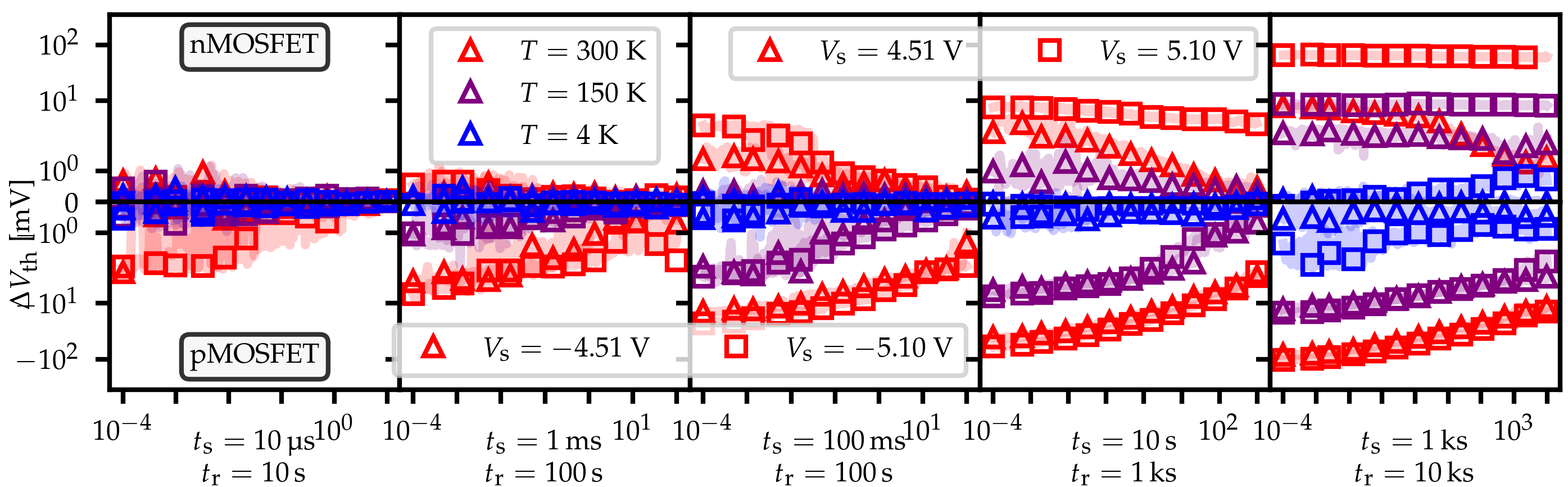
Figure 8.3: Using the eMSM method, PBTI and NBTI trends have been measured on nMOS and pMOS devices for  and two stress voltage conditions
 ![\( \vg [,s]=\pm \SI {4.51}{\volt } \)](draftv0-images/0B55521D63936CCC7123BEC0E075429B.svg) and
and ![\( \vg [,s]=\pm \SI {5.10}{\volt } \)](draftv0-images/D64225BFDEA0BB82ED1885F441447367.svg) . While at room temperature is around 100 mV for the longest stress times, BTI freezes out completely towards cryogenic temperatures. Figure taken from [MJC4].
. While at room temperature is around 100 mV for the longest stress times, BTI freezes out completely towards cryogenic temperatures. Figure taken from [MJC4].
The trap bands for this technology have been extracted by using measurement data obtained at room temperature and above [MJJ2]. The MSM curves shown in Fig. 8.2 (left) have been measured at  for three different bias conditions on nMOS and pMOS and were used to extract the trap bands with Comphy employing the ESiD algorithm presented in Section 4.2. By using two independent search regions for the algorithm, two different trap bands representing the oxide and a 0.6 nm thick interface layer (IL)
are extracted and shown in Fig. 8.4 (left). Most defects are located within the IL and exhibit trap levels approximately 1 eV
below and above the midgap of the Si substrate. The distribution of relaxation energy and trap level is in good agreement with DFT calculations, as can be seen for the hydrogen bridge (HB), hydroxyl-E’ (HE) center and oxygen
vacancy (OV) represented by the lines in Fig. 8.4. Using this extracted trap bands, the measured recovery behavior in
Fig. 8.2 (left) can be replicated by the models as shown by the solid lines. By plotting the relaxation energy against the trap level as in
Fig. 8.4 (right), it can be seen that results from earlier single-defect measurements [250, 251] shown by black crosses are in
excellent agreement with the extracted measurements.
for three different bias conditions on nMOS and pMOS and were used to extract the trap bands with Comphy employing the ESiD algorithm presented in Section 4.2. By using two independent search regions for the algorithm, two different trap bands representing the oxide and a 0.6 nm thick interface layer (IL)
are extracted and shown in Fig. 8.4 (left). Most defects are located within the IL and exhibit trap levels approximately 1 eV
below and above the midgap of the Si substrate. The distribution of relaxation energy and trap level is in good agreement with DFT calculations, as can be seen for the hydrogen bridge (HB), hydroxyl-E’ (HE) center and oxygen
vacancy (OV) represented by the lines in Fig. 8.4. Using this extracted trap bands, the measured recovery behavior in
Fig. 8.2 (left) can be replicated by the models as shown by the solid lines. By plotting the relaxation energy against the trap level as in
Fig. 8.4 (right), it can be seen that results from earlier single-defect measurements [250, 251] shown by black crosses are in
excellent agreement with the extracted measurements.

Figure 8.4: The measured curves shown in Fig. 8.2 (left) allow the extraction of a interface trap layer and an oxide trap band using the ESiD algo-
rithm. The extracted trap levels and relaxation energies (left) of the IL defects are in good agreement with DFT calculations (solid lines). The ( ,
,  ) heat map (right) for the IL trap bands shows that the extracted parameters are in good agreement with extracted parameters from single defect measurements [250, 251] represented by the black crosses. Figures taken
from [MJJ2].
) heat map (right) for the IL trap bands shows that the extracted parameters are in good agreement with extracted parameters from single defect measurements [250, 251] represented by the black crosses. Figures taken
from [MJJ2].
While the recovery curves in Fig. 8.3 show, that Tech. B freezes out completely towards cryogenic temperatures, this is not the case for Tech. A. As can be seen in Fig. 8.5 (left),
there is a high asymmetry between nMOS and pMOS devices. The points, representing measurement data show that across all stress time conditions at room temperature on nMOS is almost twice as large as observed for pMOS. This can also be seen in Fig. 8.5 (right) for a higher
temperature of  . While BTI within the pMOS device freezes out completely towards cryogenic temperatures, the nMOS device still shows a large , even at 4 K. At cryogenic temperatures, there is still a of more than 20 mV for the longest
  .
.

Figure 8.5: Tech. A shows a very asymmetric behavior of across all measured temperatures. At room temperature in the PBTI case on nMOS is twice as large as NBTI on pMOS. The latter freezes out completely below 150 K, while on nMOS there is still a of around 40 mV. Even at 4 K nMOS clearly does not freeze out but shows a relatively large shift of more than 20 mV. Figures taken from [MJJ5].
The simulations shown in Fig. 8.5 (left) as solid lines have been perforemed using Comphy in combination with the
ESiD optimization algorithm and the WKB-based approximation of the full quantum mechanical 2-state NMP transition model. For this, a grid of relaxation energies and trap levels has been spanned. This has been done for two independent trap bands for both, nMOS and pMOS (in total 4 independent bands), one trap band represents defects at the interface layer in the SiO2 and one
trap band represents defects in the HfO2 . Additionally, the grid evolves across the spatial position  and the configuration coordinate offset
  . For these two grids, the average response was computed while the least square fit has been done across and . The full set of parameters can be seen in Tab. 8.1.
| Layer |  range range |
 |
range |
 |
|
SiO |
−2 eV to 2 eV | 0.1 eV | 0.1 eV to 5.0 eV | 0.2 eV | |
| HfO |
−2 eV to 2 eV | 0.1 eV | 0.1 eV to 5.0 eV | 0.2 eV | |
| Layer |  range range |
 |
 range range |
|
|
| SiO |
0 nm to 1.0 nm | 0.1 nm | ![\( \SIrange [range-phrase=\ to\ ]{2.0}{8.0}{\sqrt {u}\angstrom } \)](draftv0-images/9D901BC5DB5C95163FD4BFE6CA08453E.svg) |
 |
|
| HfO |
1.0 nm to 3.1 nm | 0.1 nm | |
|
|
Table 8.1: The initial grid parameters of the ESiD optimization for a shallow and a deep trapband in both, the SiO-layer and the HfO-layer. The mean response of the configuration coordinate offset and the spatial position has been computed and used for the NNLS optimization of and .
Using this modeling approach allows to accurately and efficiently rebuild the measured data within the simulation, as can be seen from the lines, as can be seen in the simulated lines in Fig. 8.5 (left). The extracted trap band parameters from the simulation are shown in Fig. 8.6 (left). As was the case for Tech. B,
the interface trap bands in the SiO2 layer are roughly 1 eV above and below the Si midgap. The deep trap bands, mainly responsible for NBTI in pMOS are concentrated very close to the valence bandedge, whereas
the shallow trap bands, responsible for PBTI in nMOS are located around 300 meV above the bandedge. This can be seen also in the (,)-heatmap in Fig. 8.6 (right). There is a peak at small relaxation energies in the shallow SiO2 trapband
which typically does not result in observable at room temperature, because these defects exhibit too small charge transition times and therefore do not contribute to within the measurement window. However, at cryogenic temperatures these defects contribute to the measured threshold voltage shift.

Figure 8.6: The eMSM measurements in Fig. 8.5 (left) allow the extraction of trap bands responsible for causing the shift using Comphy and the ESiD method. The extracted distribution of trap levels and relaxation energies (left) of defects in the SiO2 interface layer and the high-κ layer show mean trap
levels of approximately 1 eV above and below Si midgap, which is in good agreement with DFT calculations. The corresponding  -heatmap (right) shows peaks at the relaxation energies around 3 eV. Figures taken from [MJJ5].
The impact of the different trap bands at different temperatures can be seen in Fig. 8.7. The total (solid lines) is composed by the caused by defects in the SiO2 layer (dotted lines) and by such causing the of the HfO2 layer (dashed lines). For nMOS at 300 K the main contribution of the total shift comes from defects in the HfO2 -layer which recover slowly. At 4 K, the impact of the HfO2 trap band is reduced. Additionally, there is a number of very fast defects in the SiO2 interface
layer. The majority of SiO2 defects recovers slower and gives thus a relevant contribution to the total shift.

Figure 8.7: The total PBTI threshold voltage shift is composed of the caused by the trap band in the SiO2 layer (dotted) and the trap band in the HfO2 layer (dashed). At 300 K (red) the main contribution comes from defects in the HfO2 layer. Very fast
interface defects in the SiO2 layer give a large shift, however, this recovers almost immediately as soon as the stress is removed. At cryogenic temperatures (blue) the impact defects in the HfO2 , which are far away from the substrate interface, is reduced and the SiO2 defects
recover slower and thus give a relevant contribution to the total . Figures taken from [MJJ5].
The described mechanisms are illustrated in Fig. 8.8 with different colors indicating the threshold voltage shift of every
defect after a stress of ![\( \vg [,s]=\pm \SI {2}{\volt } \)](draftv0-images/E589E938A9596E863403C9D060351CDF.svg) for
for  (blue and red defects give a larger contribution to than grey defects). Defects which recover immediately after removing the stress are represented by stars. As can be seen, at 300 K a contribution from very fast defects arises, but the main contribution
stems from slower defects in the HfO2 layer. At cryogenic temperatures, the charge transfer kinetics get slower and many defects in the HfO2 freeze out completely, thus, defects in the SiO2 IL and in the
HfO2 layer deliver an approximately equal contribution to the total shift. NBTI on pMOS in Fig. 8.8 (right) is dominated by defects in the SiO2 IL. The majority of
these defects freezes out and only a less significant subset of defects contributes to at cryogenic temperatures.
(blue and red defects give a larger contribution to than grey defects). Defects which recover immediately after removing the stress are represented by stars. As can be seen, at 300 K a contribution from very fast defects arises, but the main contribution
stems from slower defects in the HfO2 layer. At cryogenic temperatures, the charge transfer kinetics get slower and many defects in the HfO2 freeze out completely, thus, defects in the SiO2 IL and in the
HfO2 layer deliver an approximately equal contribution to the total shift. NBTI on pMOS in Fig. 8.8 (right) is dominated by defects in the SiO2 IL. The majority of
these defects freezes out and only a less significant subset of defects contributes to at cryogenic temperatures.

Figure 8.8: Illustration of defects contributing to the total . PBTI on nMOS (left) after of stress is dominated by slow defects in the HfO2 layer and very fast defects in the SiO2 IL, which are marked by stars. At  many defects in the HfO2 layer freeze out and the charge transition times constants of the defects in the IL get slower, resulting in equal contributions of the SiO2 and the HfO2 defect band to . NBTI on pMOS (right) is dominated by defects in the SiO2 layer. These defects freeze out towards 4 K and only a small, not significant subset of defects contributes to at cryogenic temperatures. Figures taken from [MJJ5].
The asymmetry in the curves results from the different trap levels and relaxation energies in the trap band distributions. This effect is already known from other technologies, e.g. NBTI on pMOS in [136] where the deep trap
bands responsible for NBTI is located closer to the valence band edge than the shallow trap bands leading to an asymmetry of the quantitative exhibition between NBTI and PBTI. The same effect can be seen in Tech. A as shown for two exemplary, active defects in Fig. 8.9. Compared to the donor-like defect (right), the acceptor-like defect (left) exhibits a lower classical barrier (in both cases, stress and
recovery), which in turn leads to a larger overlap of the ground state with the corresponding wave function at the same energy level of the final state. Therefore, the donor-like defect delivers a larger contribution to the total compared to the acceptor-like defect which will have smaller charge transition times.

Figure 8.9: Acceptor-like defects responsible for PBTI on nMOS (left) show lower classical barriers compared to donor-like defects responsible for NBTI on pMOS (right). This has the effect that the overlap between the vibra- tional wavefunction of the initial and the final state for the acceptor-like defect is larger than on comparable donor-like defects leading to smaller charge transition times at cryogenic temperatures. Figures taken from [MJJ5].
The charge transition times corresponding to the selected defects in Fig. 8.9 are highlighted in Fig. 8.10 for  . The majority of the charge transition times of defects in the nMOS device is smaller than those of the defects in the pMOS device. Defects with charge transition times that are accessible in the measurement window at
300 K are shifted out of it in the pMOS device at 4 K, as can be seen in the lower right corner, while on nMOS there is still a large number of defects with charge transition times below 10 ks.
. The majority of the charge transition times of defects in the nMOS device is smaller than those of the defects in the pMOS device. Defects with charge transition times that are accessible in the measurement window at
300 K are shifted out of it in the pMOS device at 4 K, as can be seen in the lower right corner, while on nMOS there is still a large number of defects with charge transition times below 10 ks.

Figure 8.10: The highlighted charge transition times for the nMOS (upper) and the pMOS (lower) figure for different gate voltages at correspond to defects shown in Fig. 8.9. Most charge transition times shown for the nMOS device are faster than
for the pMOS device leading to more active defects in the grey marked measurement window. While almost all defects of the pMOS are shifted out of the measurement window, there is still a significant number of nMOS defects
within the window at the low temperatures of 77 K and 4 K. Figure taken from [MJJ5].
The characterization of NBTI and PBTI on large area devices shows that different technologies show a different freeze-out behavior. While on Tech. B both NBTI and PBTI freeze out completely towards cryogenic temperatures, Tech. A shows significant PBTI on nMOS even at 4 K while NBTI on pMOS freezes out. This asymmetry can be modeled with the reliability simulator Comphy using defect bands which show an asymmetry in the offset of the thermodynamic trap level to the band edge and in the relaxation energies.
The measurements on large area devices characterized by employing the eMSM method in this section show continuous recovery traces. If stress/recovery measurements are performed on scaled devices, discrete steps occur, which correspond to charge transitions involving single defects, as discussed in more detail in the following section.