Charge Trapping and Variability in CMOS Technologiesat Cryogenic Temperatures
6 Time-Zero Characterization
Understanding the time-zero properties of a device under test is the basis for every variabiltiy and reliability study of a certain technology. The reason is that  (
( ) and CV curves show not only a strong dependence on drain bias or device dimensions, but also on the device temperature. The temperature dependence is caused by reduced phonon-scattering, which
increases the mobility of the charge carriers. Furthermore, the temperature-dependent shift of the Fermi-levels, the temperature dependence of the carrier distributions and the band gap also seriously affect the device
characteristics. All these effects can change the shape of () and CV curves dramatically, which has in turn a strong impact on any reliability study. The impact of the temperature on the transition curves is discussed detailed in Section 6.1, the impact on CV curves is discussed in Section 6.2.
) and CV curves show not only a strong dependence on drain bias or device dimensions, but also on the device temperature. The temperature dependence is caused by reduced phonon-scattering, which
increases the mobility of the charge carriers. Furthermore, the temperature-dependent shift of the Fermi-levels, the temperature dependence of the carrier distributions and the band gap also seriously affect the device
characteristics. All these effects can change the shape of () and CV curves dramatically, which has in turn a strong impact on any reliability study. The impact of the temperature on the transition curves is discussed detailed in Section 6.1, the impact on CV curves is discussed in Section 6.2.
Additionally, quantum mechanical effects become dominant towards cryogenic temperatures, which do not occur in the classical limit. An example for this is resonant tunneling caused by quantum dots. This effect has been measured across various MOSFET technologies and is presented in Section 6.3.
After studying the temperature dependent time-zero characteristics on large-area devices, the characteristics are studied on SmartArrays, employing thousands of devices which can be addressed digitally. This enables the study of the temperature dependence of the variability of parameters which are an important measure for the MOSFET performance of the devices. This has been done for two different SmartArray generations with various geometries. The results are presented in Section 6.4.
6.1 Transfer Characteristics
The most widely used method for device characterization is the analysis of the () curve of a single MOSFET. This can be done for a pristine or a stressed device and allows the extraction of important quantities which determine the quality and performance of a MOSFET. To record an () curve,  is kept constant, while is swept from deep depletion to inversion. From the recorded () curve it is possible to extract multiple quantities like sub-threshold swing
  , threshold voltage
  , on-state current
  , transconductance
  , or leakage current
  , as shown in Fig. 6.1. All these parameters depend not only on the device dimensions, but also show a strong temperature
dependence as can be seen by a comparison of the ()-curve for 4 K and 298 K in Fig. 6.1. Depending on the examined quantity, () curves are plotted on a logarithmic scale (particularly for subthreshold quantities) or on linear scales as can be seen in Fig. 6.1
(right). The temperature dependence of the transfer characteristics can be seen for Tech. A in Fig. 6.2 (top) and Tech. B in Fig. 6.2 (bottom) for both, nMOS and pMOS. Towards 4 K the () curve becomes steeper and the threshold voltage and on-state current increase.
, as shown in Fig. 6.1. All these parameters depend not only on the device dimensions, but also show a strong temperature
dependence as can be seen by a comparison of the ()-curve for 4 K and 298 K in Fig. 6.1. Depending on the examined quantity, () curves are plotted on a logarithmic scale (particularly for subthreshold quantities) or on linear scales as can be seen in Fig. 6.1
(right). The temperature dependence of the transfer characteristics can be seen for Tech. A in Fig. 6.2 (top) and Tech. B in Fig. 6.2 (bottom) for both, nMOS and pMOS. Towards 4 K the () curve becomes steeper and the threshold voltage and on-state current increase.

Figure 6.1: The schematic () curves for 298 K and 4 K show a strong temperature dependence which influences various important device parameters, such as the on-current , the subthreshold swing  , the leakage current , the (maximal) transconductance
  , or the threshold voltage which can be defined at a constant current
  or with the maximum transconductance
  .
.

6.1.1 Subthreshold Swing
The steepness of the () is well-know as sub-threshold slope and is central for the switching between ON-state and OFF-state of a transistor and thus an essential performance criterion. For device characterization often the reciprocal
value is used, which is known as subthreshold swing . In the classical limit, the is defined in the weak inversion regime and given by [220]

where  is the capacitance of the oxide,
  the depletion capacitance and
  the capacitance of the interface states. The factor
  which is defined by the capacitances is often called subthreshold-swing factor. The minimal value for at a certain temperature is reached in the limit
  ,
,  and
and  . Experimentally, can be extracted using a linear fit for the subthreshold region of the logarithmic () curve. By doing so the temperature dependence of can be extracted from () measurements, and is shown in Fig. 6.3.

Figure 6.3: At temperatures above around 150 K, the subthreshold swing follows the Boltzmann relation (black line). Towards cryogenic temperatures it starts to saturate which can be seen for pMOS (left) and nMOS (right). This behavior has been observed for various technologies and can be explained by band tail states [110].
According to the classical Boltzmann thermal limit is defined as  . Here, is the subthreshold-slope factor which can be approximated by
  with
with  being the surface potential. The classical Boltzmann thermal limit is experimentally not accessible below around 100 K, but starts to saturate towards a constant value. This can be seen in Fig. 6.3 for Tech. A for pMOS (left) and nMOS (right). This
saturation effect of the subthreshold swing has been measured across multiple different FET technologies as shown in [110]. The deviation from the Boltzmann thermal limit can be explained by band tail states near the interface
between the substrate and oxide. These band tail states occur for example due to static or dynamic disorder from interface defects, impurities or electron-phonon scattering and lead to a blurred band edge. This can be modeled
precisely using Gauss hypergeometric functions for the band tails [221]. However, these functions require a large computational effort compared to a simplified model using exponential band tails
being the surface potential. The classical Boltzmann thermal limit is experimentally not accessible below around 100 K, but starts to saturate towards a constant value. This can be seen in Fig. 6.3 for Tech. A for pMOS (left) and nMOS (right). This
saturation effect of the subthreshold swing has been measured across multiple different FET technologies as shown in [110]. The deviation from the Boltzmann thermal limit can be explained by band tail states near the interface
between the substrate and oxide. These band tail states occur for example due to static or dynamic disorder from interface defects, impurities or electron-phonon scattering and lead to a blurred band edge. This can be modeled
precisely using Gauss hypergeometric functions for the band tails [221]. However, these functions require a large computational effort compared to a simplified model using exponential band tails  , as can be seen in Fig. 6.4, which is derived in detail in [MJJ4].
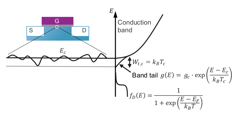
Figure 6.4: Crystalline disorder leads to blurred band edges. These can be modeled assuming exponentially decaying band tail states depending on a critical temperature  . This widened band edge contribute to the energy scan by the Fermi distribution and can explain the saturation of the subthreshold slope. Figure taken from [MJJ4].
As shown by Beckers et al. [MJJ4] the introduction of a critical temperature  , which is typically around 30 K to 50 K, allows the adaption of the classical to

with


and
![(6.5) \{begin}{align} y=\exp \left [(1-\theta )\big (\frac {x}{k_\mathrm {B}T}\big )\right ]. \{end}{align}](draftv0-images/image-604.svg)
In this closed form expression  is the energetic offset between the conduction band and the Fermi level and
  . This closed-form simplification of the model presented in [221] describes the temperature dependence of and the occurring saturation efficiently and is thus well suited for usage in commercial device simulators.
6.1.2 Transconductance
The transconductance (short for transfer conductance) relates the drain current with the gate voltage via

at a constant . Towards lower temperatures, electron-phonon scattering gets reduced, leading to a higher carrier mobility. This has the effect of an increasing transconductance, as can be seen in Fig. 6.5 for Tech. A for both pMOS (left) and nMOS (right). The
overall shape of gets steeper because the Fermi-Dirac distribution becomes narrower at low temperatures. The point of maximum which also gets continuously larger for lower temperatures, as can be seen in Fig. 6.5 (bottom), is widely used for the definition of the
threshold voltage, as discussed in the upcoming section in detail.

Figure 6.5: The shape of the transconductance shows a strong temperature dependence for both pMOS (left) and nMOS (right) of Tech.
A. The steeper and sharper at 4.2 K can be explained by the sharper Fermi-Dirac distribution at cryogenic temperatures; increases at lower temperatures because the mobility increases due to reduced phonon-scattering.
It has to be noted that the characteristics shows a maximum for each transistor. The point of can become degraded due to higher contact resistance or an increase in the number of interface states. The latter affect , because the mobility of the carriers reduces due to Coulomb scattering at interface defects. This effect is deliberately used to link a decreasing to an increasing concentration of interface defects [180].
6.1.3 Threshold Voltage
The threshold voltage of a MOSFET is the minimal gate voltage which needs to be applied to turn the device on, which means creating a conduction path between source and drain [220]. While or transconductance are well defined, there are multiple definitions for the threshold voltage. In this work, two different methods for extracting the threshold voltage from measurements will be used: The constant
current method and the  method, referred to
  and
and  , respectively. For the constant current method, a constant current is defined at which the corresponding threshold voltage is extracted, as can be seen in Fig. 6.1(a). For the method the point of is extracted. Then the intersection point of the tangent line with
  is found. The corresponding voltage is defined as .
An extraction of and is shown for Tech. A in Fig. 6.6 for
pMOS (left) and nMOS (right). As can be seen, with the two methods not the same threshold voltage values are extracted, in fact, they do not even exhibit the same temperature dependence. In the case of pMOS, decreases by approximately 350 mV while decreases only by approximately 200 mV when the temperature is changed from 300 K to 4 K. Even worse is the difference for nMOS. Here not only a difference in the absolute shift, but
also a change of the shape for the T-dependence can be observed. While for pMOS the T-dependence is almost perfectly linear, the nMOS device shows a saturation of the threshold voltage, which is stronger for than for . This rather complex T-dependence of the different definitions is discussed in detail in [111]. By discussing the impact of the temperature dependence of the bulk Fermi potential, dopant freezeout, field-assisted dopant ionization, bandgap widening and interface
traps, Beckers et. al. model and show that the saturation of for nMOS towards 4.2 K can be explained by the presence of interface defects in combination with the shift of the bulk Fermi potential [111].

Figure 6.6: The threshold voltage increases towards cryogenic temperatures for both nMOS and pMOS of Tech. A. Different defini-
tions and extraction methods of lead to a different T-dependence which is discussed in detail in [111].
The threshold voltage plays an important role for the evaluation of the reliability of a certain technology. It is often used as reference before applying stress to a device. During stress the shape of the () curve can change, which is often simplified by assuming a parallel shift of the whole () curve. The change in extracted from the initial and stress device is often compared. For this, needs to be extracted from the () which makes it necessary to decide on a certain definition. These methods are discussed in detail in the upcoming sections about reliability characterization.
6.1.4 ON-State Current
The ON-state current is extracted in the saturation region, typically at  . for Tech. A pMOS (left) and nMOS (right) can be seen in Fig. 6.7, extracted at
  and
and  , respectively. As can be seen,
  decreases for pMOS and increases for nMOS with decreasing temperatures, which can be explained by the increasing mobility of the charge carriers. This means that at cryogenic temperatures the efficiency of
MOS devices increases, which is beneficial for the performance of circuits at these temperatures.
decreases for pMOS and increases for nMOS with decreasing temperatures, which can be explained by the increasing mobility of the charge carriers. This means that at cryogenic temperatures the efficiency of
MOS devices increases, which is beneficial for the performance of circuits at these temperatures.

Figure 6.7: The ON-current of Tech. A decreases for pMOS (left) and increases for nMOS (right) towards 4.2 K. This can be explained by the increasing mobility due to reduced phonon-scattering.