The modern world is brimming with micro- and nanoscale devices. Whether semiconducting logic [1] or memory devices [2] at the core of modern computing systems, optical or optoelectronic devices in
communications [3] and quantum science [4], or microelectromechanical systems (MEMS) sensors in aviation [5], there is no facet of society which has not been transformed by these advanced technologies.
However, the continuing advancement of micro- and nanotechnology requires ever more complex manufacturing, with modern semiconductor fabrication facilities nowadays sometimes requiring investments in the order of tens of
billions of dollars [6].
With such enormous resources involved, the development of new technologies cannot depend only on experimental pathfinding, since the experiments can be very complex and costly, and the design space is too vast [7].
Therefore, simulation tools are fundamental as a cost-saving and insight-producing measure. Over the decades, the field of technology computer-aided design (TCAD) has emerged to address the issue of development and application
of computational models to simulate the fabrication and operation of semiconductor devices and circuits [8].
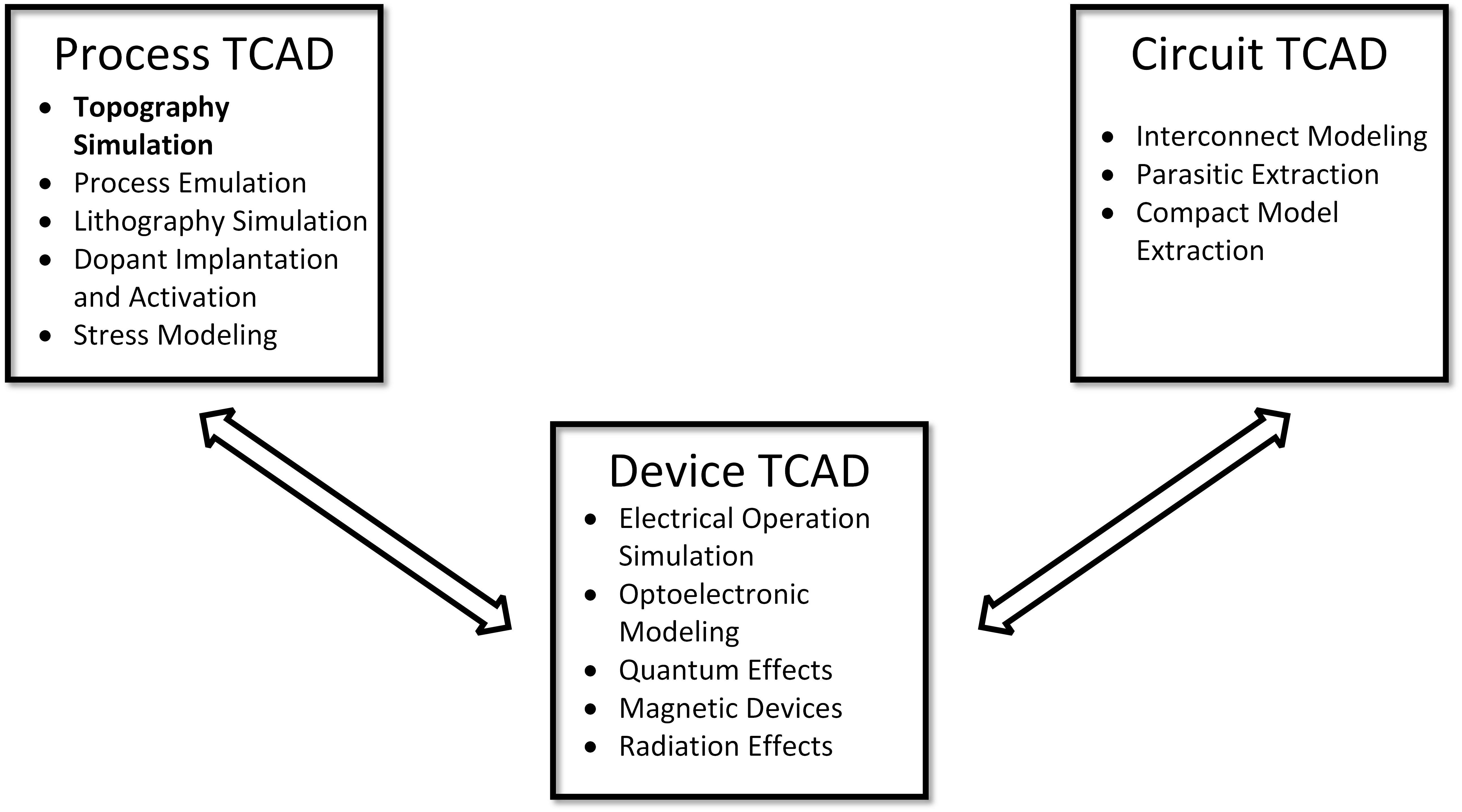
TCAD contains several sub-fields which can be broadly gathered into three distinct categories, as illustrated in Fig. 1.1. At the center is device TCAD which concerns itself with
simulating device operation [9]. Device TCAD concerns itself not only with the simulation of current vs. voltage characteristics, but also includes, e.g., the sub-fields of modeling of optoelectronic devices [10],
quantum effects [11, 12], magnetic devices [13], and the effects of radiation [14].
Multiple devices can be interconnected to form an electrical circuit, and its characteristics can be simulated with circuit TCAD. The categories of device and circuit TCAD are intrinsically linked, since, e.g., the electrical
characteristics obtained from device TCAD can be used to construct compact models which more efficiently enable the simulation of connected devices [15]. Additionally, circuit TCAD encompasses the modeling of the
interconnects linking multiple devices [16] and the extraction of parasitic parameters [17].
Figure 1.1: Illustration of the three main categories of TCAD including related sub-fields.
The third category is dedicated to modeling and simulation of the fabrication processes of semiconductor devices. This category is called process TCAD, and this thesis situates itself broadly within its scope. Both
historically [18] and more recently [19], these simulations have attracted major research and industrial attention.
This is because they stand at the beginning of the chain of TCAD investigations. Process TCAD is a fundamental enabler of modern micro- and nanodevices, since it not only provides physically realistic structures for device
simulation, but also directly deals with the most costly aspect of the semiconductor value chain [20, 21]: The manufacturing process.
There are several processes required for the manufacturing of a modern semiconductor device, all of them requiring attention from process TCAD. Historically, substantial development attention has been placed on processes which
directly impact the electrical characteristics of the devices, such as dopant implantation [22] and diffusion [23], as well as oxidation [24] and stress accumulation [25]. Since the desired outcome is the study
of electrical phenomena, comparatively little attention had been paid to the precise shape of the devices.
More recently, however, precise control of the final shape of the processed device has become a more salient issue [26]. The increased miniaturization of devices has led to the development of non-planar structures such as fin
field-effect transistors (FinFETs) and gate-all-around (GAA) transistors which have decreased tolerances and require more control of the fabrication processes [27]. Also, the MEMS and nanoelectromechanical systems
(NEMS) revolution involves systems where the shape is at the forefront [28], and the emergence of superconductor electronics requires high authority over the involved Josephson junctions [29]. Thus, the sub-field of
topography simulation has garnered increase importance, since it concerns itself with the simulation of processes which dictate the final shape, i.e., the topography, of the device.
There are several processes which impact the final device structure. Centrally, there are the complementary processes of deposition [30] and etching [31], i.e., the addition and removal of material,
respectively. These processes can be further described according to the specificities of the involved reactor. For example, the deposition of material in a vacuum reactor through physical processes is called physical vapor deposition
(PVD) [32], while the deposition exploiting chemical reactions is named chemical vapor deposition (CVD) [33]. In etching, there is a broad distinction between liquid-phase reactors, named wet etching, and vapor- or
plasma-phase processes, called dry etching [7].
Etching and deposition are not the only processes which affect the structure. For example, chemical-mechanical planarization (CMP) [34] and oxidation [35] have a severe impact on the final shape. Additionally, there is
the process of lithography, i.e., the printing of patterns on photoresist material through light [36]. However, due to its specialized nature, lithography modeling is often considered a separate sub-field [37]. The
simulation of the involved reactors is also a separate domain of expertise [38].
Since the simulation of the reactors is not directly involved in conventional topography simulation, two different geometrical scales can be naturally defined. The reactor-scale involves the entire reactor, focusing on, e.g., the
generation of active reactants, as well as their characteristics and distributions across the entire wafer [38]. Topography simulation operates, instead, at the feature-scale, where only a small region of interest is
investigated. Small regions are, for example, a single transistor [39], an individual MEMS structure [40], or even somewhat larger structures such as three-dimensional (3D) NAND channel holes [26]. These two
regions are linked by an abstract region of the feature-scale named the source plane, where the outputs of a reactor-scale analysis, such as reactant species incoming angular distribution functions, become fixed inputs for the
topography simulation.
Topography simulation is composed of two major elements. First, it must be able to robustly describe evolving surfaces. This is particularly challenging for the aforementioned processing techniques since changes in the topology can
occur. For example, during etching, a layer might be completely pierced; or a hole might be covered leaving an air-gap during deposition. These changes are exceedingly challenging to model using conventional explicit surface
representations such as polyhedral meshes [41]. Therefore, implicit surfaces and, crucially, the level-set (LS) method have emerged as the standard surface representation and advection method, respectively, for topography
simulation [42].
In addition to the surface representation, the second major element is the determination of the surface advection velocity distribution. In other words, the physical and chemical phenomena involved with the distribution of
reactants, i.e., the reactive transport, must be modeled. Reactive transport modeling entails the calculation of the trajectories of particles through the simulation domain as well as their interaction with the evolving
surface. Such particles can directly represent the reactant species and the respective chemical interactions. However, a particle can also be an aggregate of several reactants into a single representation. This is often the case for
processes involving plasmas [43], since the involved chemistry is not only complex but also often unknown.
For example, several polymerizing species can be aggregated into an effective particle which represents the formation of the polymer protective film in reactive ion etching (RIE).
Nonetheless, if a precise reactor model is available and the possible physical and chemical reactions are known, the reactive transport can in principle be directly modeled [44]. In practice, however, this is exceedingly difficult.
Even for very established processes, there is still a very active scientific debate over the involved surface phenomena [45]. Additionally, the reactors, in particular those involving plasmas, are exceptionally complex, therefore,
predictive modeling is not always possible.
This motivates the development of phenomenological models. That is, models which attempt to capture the most essential phenomena known from physical-chemical intuition [46]. Since these models are intrinsically
simplified, they necessarily involve parameters which must be calibrated to experimental data. Nevertheless, if these models are properly justified, the extracted parameters can be meaningful and, thus, shine light into the
processing conditions. Therefore, in the spirit of Occam’s Razor [47], a phenomenological model must be constructed as parsimoniously as possible to adequately capture reality. Phenomenological modeling is fundamentally
different to process emulation [48], where the geometric properties gathered from experiments are directly described without involving physical insight. This direct description of properties is also named
geometrical modeling.
In this attitude of simplicity, a further subdivision are the so-called single-particle models. In them, the entire physical and chemical complexity of the reactants is abstracted into a single representative phenomenological
species, whether representing a chemical species or a phenomenological aggregate. Although for some processes a larger number of phenomenological particle species are necessary even for the simplest possible model [43], for
several others a single-particle representation is sufficient. In fact, from the point of view of phenomenological modeling, a simpler model with fewer species is more desirable, since more information can be gained from the
parameters.
The choice of a minimal number of species requires deep knowledge of the involved processing step. In general, single-particle models are adequate for processes where one chemical species is the limiting factor, even if different
species might be involved in the reaction. For example, low-bias plasma etching [49], atomic layer processing (ALP) in the single-reactant limited regime [30], CVD [50], and PVD [51] are ideal applications
to phenomenological single-particle modeling.
1.1 Research Goals
The research goals of this thesis are, in summary, the development of sufficiently accurate phenomenological single-particle reactive transport models for topography simulation and their application to relevant etching and
deposition processes. These models must be robust enough to be accurate without resorting to reactor or first-principle calculations. Simultaneously, the number of parameters should be kept as low as possible to maximize their
chemical interpretability.
With robust and accurate models, direct modeling, i.e., the reproduction of experimental topographies, is possible. This enables the generation of physically-sound device structures which are of great importance to device engineers.
In addition, a phenomenological model should enable inverse modeling: The extraction of useful chemical information from experimental topographies. Finally, the application of these models must be able to provide
experimentally-actionable input to process developers, that is, phenomenological modeling must be demonstrated as a constituent of a larger optimization effort.
Research Setting
The research presented in this thesis has been conducted within the scope of the Christian Doppler Laboratory for High Performance TCAD at the Institute for Microelectronics, TU Wien. This Laboratory is a long-term
collaboration pursuing application-oriented basic research between the Institute for Microelectronics and Silvaco Europe Ltd., a leading commercial provider of electronic design automation (EDA) and TCAD tools, jointly funded
by the Christian Doppler Association and the involved company. The Laboratory is led by Prof. Josef Weinbub.
The research collaboration regarding low-bias sulfur hexafluoride (SF6) plasma etching of silicon (Si) for microcavity resonators has been established in collaboration with the experimental teams led by Prof. Ulrich
Schmid of the Institute of Sensors and Actuator Systems, TU Wien, and by Dr. Michael Trupke of the Vienna Center for Quantum Science and Technology (VCQ) at the Faculty of Physics, University of Vienna. The computational
results in Chapter 6 were obtained using resources from both the Vienna Scientific Cluster (VSC) and from the computing infrastructure of the Institute for Microelectronics.