Chapter 6 Optimization of Silicon Microcavity Resonators
The final technical chapter of this thesis focuses on an application of topography simulation to the optimization of a fabrication process. As previously discussed in Chapter 5, the top-down
single-particle flux modeling approach with constant sticking coefficient \(\beta _\mathrm {eff}\) is adequate for low-bias sulfur hexafluoride (SF6) plasma etching of silicon (Si). Therefore, attention can now be
placed on the optimization of an actual device component manufactured using this process: Silicon microcavity resonators. These components are under active investigation by experimental collaboration partners at the University
of Vienna and TU Wien [168, 188], and they can be further optimized by achieving a higher degree of control of the microcavity shape.
Optical resonators are a fundamental component of modern light-based devices with diverse applications [189]. The resonator quality strongly depends on the exact shape of the involved microcavities [187]. Therefore,
their optimization requires achieving fine control over the geometry which subsequently involves a large effort in understanding their manufacturing. Conventionally, microcavities are manufactured in Si wafers using isotropic wet
etching [190, 191]. More recently, low-bias SF6 plasma etching has been introduced as an alternative to this method due to its improved controllability, uniformity, and reproducibility [49]. Even though
many advances have been made to reduce surface roughness [180] and improve mirror alignment [168], the challenge of precisely controlling the shape of the cavity still remains.
Topography simulation is an invaluable tool to tackle the issue of shape control. It is able to not only precisely reproduce the experimental geometries, but also enables a detailed investigation of alternative process recipes without
having to perform multiple costly experiments. This chapter presents a simulation-driven optimization of the process parameters, namely the etch times, based on a robust calibration procedure. First, the fabrication and
characterization of the experimental microcavity, performed by the collaboration partners, is briefly reviewed. Then, a robust novel calibration procedure is discussed, with particular focus on the critical feature detection algorithm.
Finally, having obtained a calibrated simulation, the extraction and optimization of the microcavity parameters is presented.
Own contributions: The development of the custom feature detection algorithm, its integration with an automatic calibration procedure, and also the computational study of the optimization of optical and process
parameters are novel contributions. These results have been originally published as a journal article [174].
6.1 Silicon Microcavity Resonators
Optical resonators are invaluable components with applications in diverse fields of science and technology. They enable a strong coupling between matter and light, thus finding use in, e.g., laser physics [192, 193],
spectroscopy [194, 195], and in fundamental quantum science [196, 197]. There are several mirror configurations which enable optical resonators [168, 187], but in general they involve at least one cavity. For
instance, a plano-concave (PC) resonator requires one cavity and one plane mirror, while a concave-concave (CC) configuration requires two cavities. In all cases, a very precise control of the shapes of the cavities is crucial, since
geometric quantities, such as the radius of curvature (ROC), directly impact the quality metrics of the resonator [187].
Advanced micro- and nanomachining techniques of Si lend themselves to the development of very high quality optical resonators based on silicon microcavities. Since the desired structures have spherical or parabolic shapes, i.e.,
broadly isotropic shapes, the initial research efforts were driven by conventional isotropic wet etching of Si [190, 191]. However, as discussed in Chapter 5, low-bias plasma etching using
SF6 gas can have several advantages regarding controllability, reproducibility, and uniformity [49]. In addition, as shown in Section 5.2, an ideally
isotropic process can lead to perfectly flat regions which are detrimental to optical device performance, since in this case the ROC is infinite.
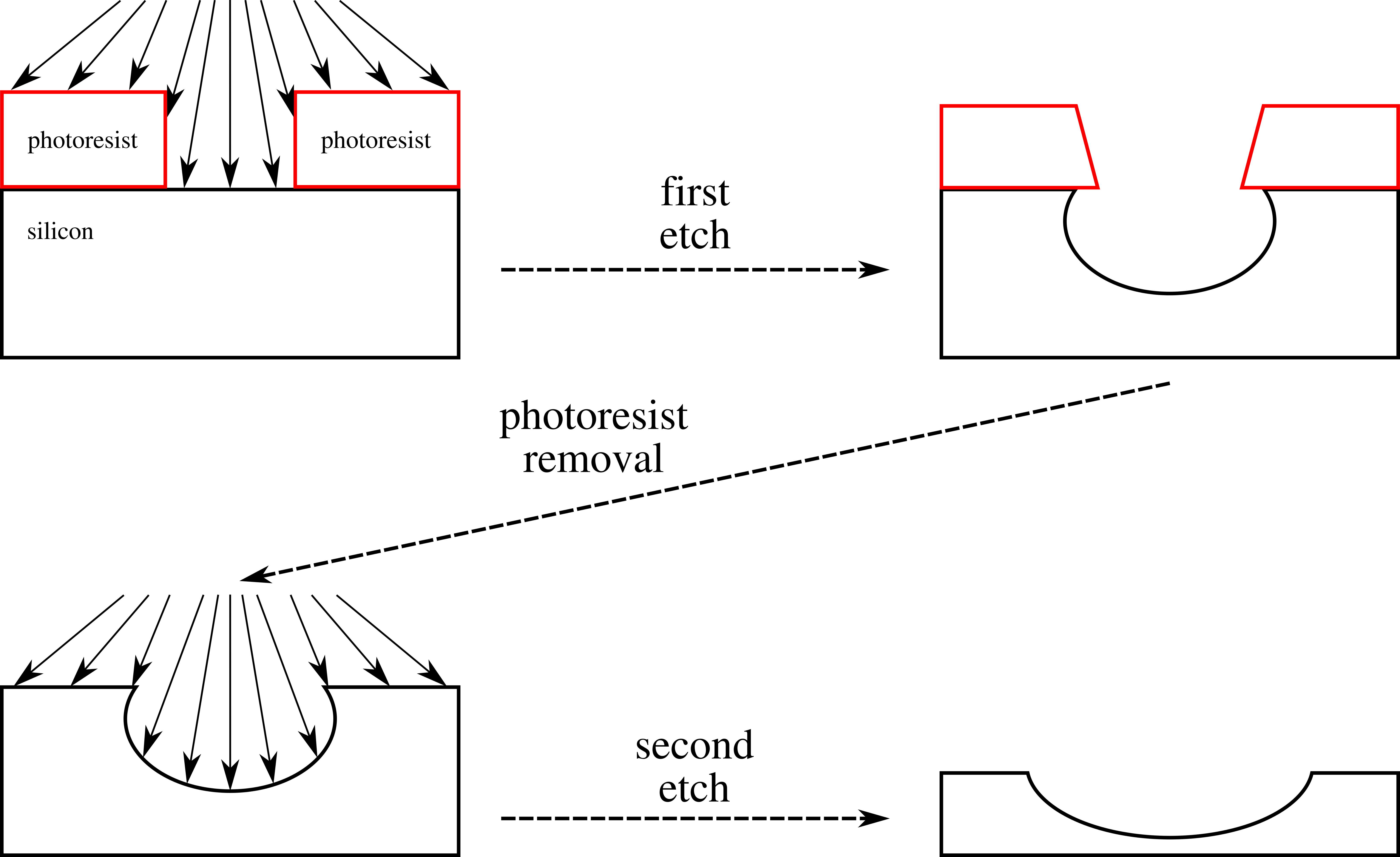
A two-step low-bias inductively couple plasma (ICP) etching of Si has thus been proposed by Larsen et al. as a dry alternative to wet etching configurations for silicon microlens mold fabrication [49]. This fabrication
process is illustrated in Fig. 6.1. After cylindrical openings are lithographically patterned on the photoresist, a first etch step is performed. The photoresist is then removed,
and a second etch step is executed. This second maskless step is proposed to improve the quality of the final structure, a claim which is evaluated in Section 6.4. One
significant trade-off of this approach is the increase in surface roughness [179] which is typical of dry etching processes. However, this roughness can be mitigated by a series of oxidation and oxide removal steps [180].
Additionally, SF6 etching enables the use of deep reactive ion etching (DRIE) techniques to create alignment structures which are crucial to enable high quality CC resonators [168].
This two-step etching process is employed by the experimental collaboration partners from the University of Vienna and TU Wien, first described by Wachter et al. in [168]. A moderately doped, \(n\)-type
Si(\(100\)) wafer is used as a substrate. Three layers of AZ6624 photoresist are added to achieve a masking layer thickness of \(\SI {9}{\micro \meter }\).
The resist is then lithographically patterned with an array of \(100\) cylindrical holes with diameters \(d\) homogeneously increasing between \(\SI {12.4}{\micro \meter }\) and \(\SI {52}{\micro \meter }\). Both etch
steps are performed in the same ICP reactor using SF6 gas at a flow rate of \(\SI {100}{\sccm }\), a coil power of \(\SI {2}{\kilo \watt }\), and a table power of \(\SI {15}{\watt }\). The first etch step is
performed for \(\SI {320}{\second }\), and the second is performed for \(\SI {48}{\minute }\). Between the etch steps, the photoresist is completely striped using acetone. A polishing step, consisting of wet oxidation of Si to
a thickness of \(\SI {2}{\micro \meter }\) followed by oxide removal using a solution of hydrogen fluoride (HF), is performed twice.
From the \(100\) fabricated microcavities, three representative initial diameters are selected for analysis: The smallest (\(\SI {12.4}{\micro \meter }\)), the largest (\(\SI {52}{\micro \meter }\)), and an intermediate value
(\(\SI {34}{\micro \meter }\)). After the polishing procedure, their topographies are measured using a white light profilometer. Since there are steep angles near the edges, there is some lost information due to reflection. To
partially recover this information, an additional tilted profilometer measurement is performed. All of these measurements are realized by the collaboration partners.
Then, these measurements were processed and tilt-corrected using the open-source tool Gwyddion [198]. Both profilometer measurements are combined into a single coordinate list for each microcavity after matching the
cavity centers to the same \((x,y)\) position. In order to reproduce these measurements and to explore the process parameter space, topography simulations using the level-set (LS) method are performed.
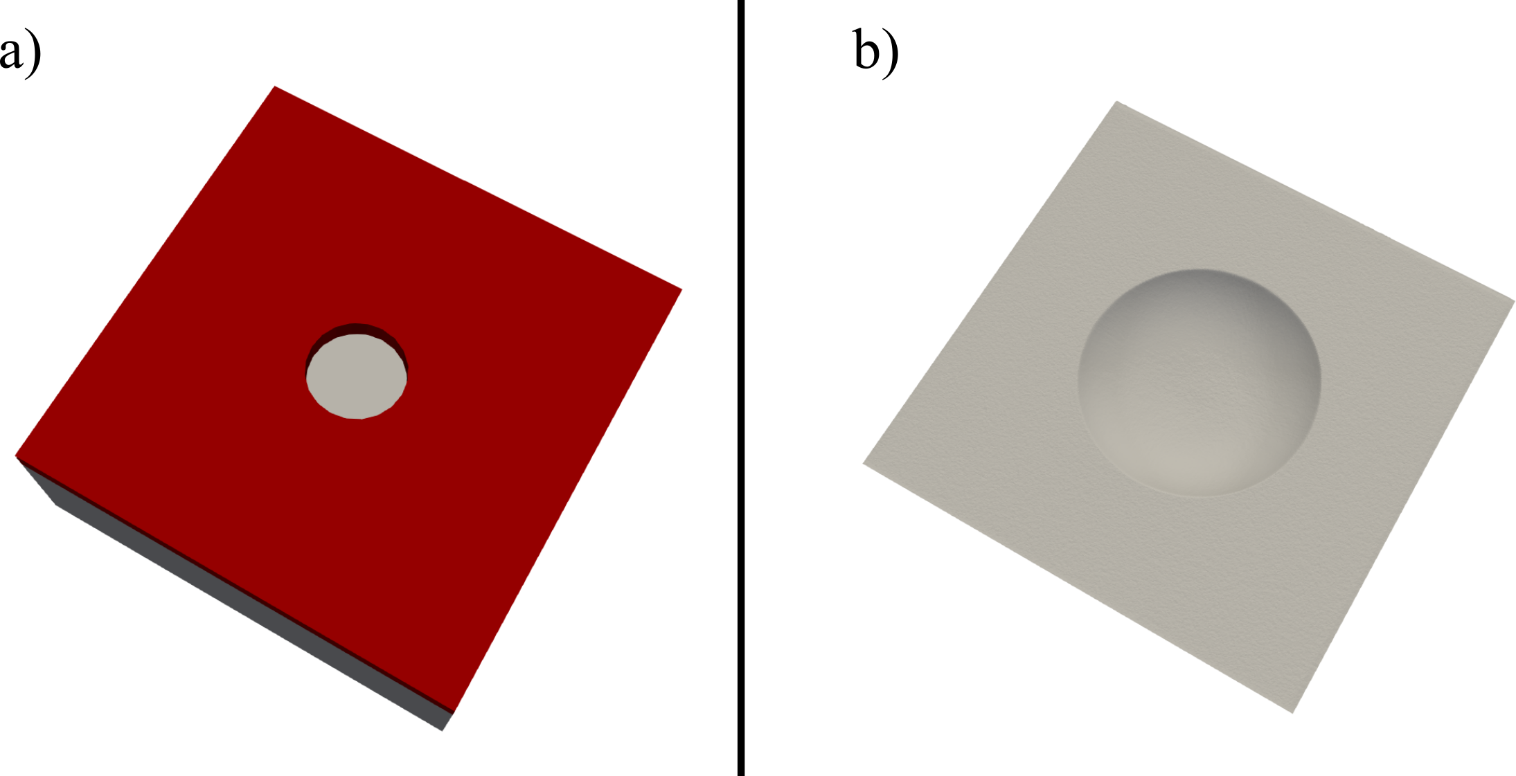
This physical simulation focuses on the most important aspects of the fabrication processes, namely the two etch steps. The simulation assumes as the starting point an ideal lithography process, illustrated in Fig. 6.2.a). The etch steps are both physically modeled with the top-down flux modeling approach, described in Section 2.3.3 and evaluated in
Section 5.2, while the photoresist removal is assumed to be ideal and, thus, performed geometrically. The final state of the surface after both etch steps is shown in Fig. 6.2.b).
The topography simulation attempts to follow the physical process as closely as possible. The initial state of the geometry is a photoresist including an ideal cylindrical hole and a thickness of \(\SI {9}{\micro \meter }\) placed
on top of a \(\SI {160}{\micro \meter } \times \SI {160}{\micro \meter }\) slab of Si. The etch times are taken directly from the experimental data. Since the mask removal step is assumed to be ideal, after the first etch
step the photoresist is geometrically removed. Any noise present in the simulation is strictly numerical due to the finite number of Monte Carlo samples and does not represent the physical surface roughness. The slight additional
etching resulting from oxidation and oxide removal in the polishing procedure is captured by artificially increasing the etch rate for the second etch step. The simulations are performed using the topography simulator
ViennaTS [57]. At the end of a simulation run, the LS surface is converted to a triangle mesh using the VTK format [199] which is then used for calibration and parameter analyses presented in the following sections.