Previously, a feature-scale model of SF6 etching of Si has been proposed [182]. This model achieved good agreement with experiments by including a very accurate model for the ion energy and angular
distribution functions. However, this description of the angular distribution functions is more relevant for high-bias applications since it plays a key role in determining the anisotropy. Additionally, said model is strictly
two-dimensional (2D), therefore unable to differentiate between trenches and cylindrical holes which, as discussed in Chapter 3, can significantly impact the final geometry.
Thus, a fully three-dimensional (3D) model is necessary. In the context of phenomenological modeling, the goal is to determine the simplest possible model which is able to satisfactorily reproduce the experimental topographies.
Then, having determined the suitable phenomenological model, it is possible to interpret it with respect to the physical processes and the involved parameters. To that end, the following approaches to calculate the local fluxes, first
introduced in Section 2.3, are evaluated in comparison to experimental data: Constant flux, bottom-up visibility calculation, and top-down pseudo-particle tracking.
In all cases, only a single particle is considered. However, unlike the discussion in Chapter 4, this particle is not interpreted as representing a distinct chemical species. There is still debate
about the precise mechanism of etching [45], although some recent first-principle studies highlight the role of SF5+ and SF\(_n\) (\(n \le 6\)) radicals [183]. Instead, the particle is assumed
to be an aggregate of etchants with similar properties, in what is conventionally named as "neutrals" [43, 134].
For the top-down approach, constant and effective sticking coefficient \(\beta _\mathrm {eff}\) approximation from Eq. (2.18) is assumed.
Since the etching process is nearly isotropic, the resulting features do not involve high AR. Therefore, no approximate one-dimensional (1D) model is available for evaluation. For the calculation of the surface evolution, these
approaches are integrated with level-set (LS) based topography simulators: Silvaco’s Victory Process [55] and the open-source simulator ViennaTS [57].
The calibration and evaluation of the flux modeling approaches are done with respect to 3D optical profilometer data of etched microcavities provided by collaboration partners from the University of Vienna and TU Wien, first
reported in [168]. In their experiment, multiple cavities with different initial photoresist cylindrical openings \(d\) were simultaneously etched in a two-step process under the reactor conditions reported in Tab. 5.1 under "Wachter et al. 2019". The first etch step was performed with the photoresist mask present for an etch time of \(\SI {320}{\second }\). Afterward, the photoresist
was removed using acetone. Then, a second etch step was performed for \(\SI {48}{\minute }\). The resulting microcavities were characterized with a white light profilometer after cleaning and polishing. The optical device, its
manufacturing and subsequent analyses are presented in more detail in Chapter 6.
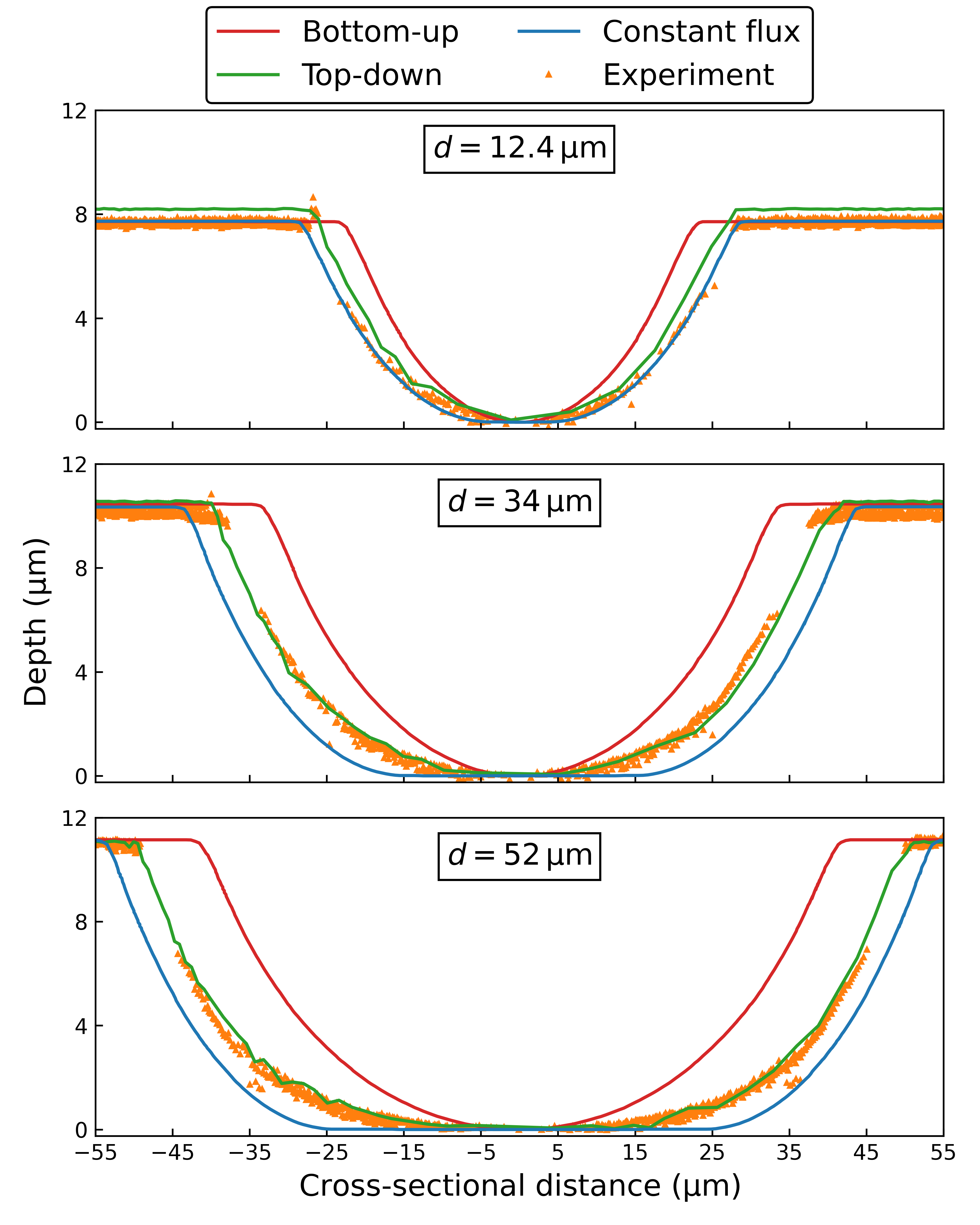
For the evaluation of the flux modeling approaches, three representative cavities are chosen, with \(d\) values of \(\SI {12.4}{\micro \meter }\), \(\SI {34}{\micro \meter }\), and \(\SI {52}{\micro \meter }\). That is,
they are the smallest, intermediate, and largest cavities available from the \(100\) cavities etched on the same chip. The calibrations are performed using the normalized flux convention from Eq. (2.7), i.e., the main calibration parameters are the plane-wafer etch rate \(\mathit {PWR}_{\mathrm {Si}/\mathrm {resist}}\) for each individual material and each etch
step. The top-down approach has as additional parameters the material-dependent constant sticking coefficients \(\beta _{\mathrm {Si}/\mathrm {resist}}\). For the top-down approach, the parameters are automatically
calibrated with the methodology described in Section 6.2 and are shown in Tab. 5.2. To obtain the clearest possible
comparison for the bottom-up and constant flux approaches, the first step \(\mathit {PWR}_\mathrm {Si}\) is manually adjusted to obtain the best possible fit, requiring a different value for each microcavity reported in Tab. 5.3. The second step \(\mathit {PWR}_\mathrm {Si}\) and \(\mathit {PWR}_{\mathrm {resist}}\) values from Tab. 5.2 are
used in all simulations. A cross-section of the simulated topographies in comparison to the profilometer data is shown in Fig. 5.1.
Implicitly, the bottom-up and constant flux approaches assume the phenomenological surface models of \(\beta =1\) and \(\beta \to 0^+\), respectively, as discussed in Section 2.3. As can be seen in Tab. 5.3, these flux approaches require a different fitted value of \(\mathit {PWR}_{\mathrm {Si}}\)
for each \(d\). This is an indication that the implied phenomenological surface models do not capture the underlying physical reality since, in principle, there is no physical explanation for starkly differing \(\mathit {PWRs}\) in
features on the same chip.
.
Parameter
Calibrated value
First etch step \(\mathit {PWR}_{\mathrm {Si}}\)
\(\SI {2.15}{\micro \meter \per \minute }\)
Second etch step \(\mathit {PWR}_{\mathrm {Si}}\)
\(\SI {0.66}{\micro \meter \per \minute }\)
\(\mathit {PWR}_{\mathrm {resist}}\)
\(\SI {0.21}{\micro \meter \per \minute }\)
\(\beta _{\mathrm {Si}}\)
\(7.5\,\%\)
\(\beta _{\mathrm {resist}}\)
\(6.1\,\%\)
Table 5.2: Parameters for top-down simulation of SF6 etching of Si microcavities automatically calibrated to experimental data.
.
\(d\)
Constant flux, first step \(\mathit {PWR}_{\mathrm {Si}}\)
Bottom-up, first step \(\mathit {PWR}_{\mathrm {Si}}\)
\(\SI {12.4}{\micro \meter }\)
\(\SI {1.45}{\micro \meter \per \minute }\)
\(\SI {23}{\micro \meter \per \minute }\)
\(\SI {34.0}{\micro \meter }\)
\(\SI {1.94}{\micro \meter \per \minute }\)
\(\SI {6.0}{\micro \meter \per \minute }\)
\(\SI {52.0}{\micro \meter }\)
\(\SI {2.09}{\micro \meter \per \minute }\)
\(\SI {3.6}{\micro \meter \per \minute }\)
Table 5.3: First step plane-wafer Si etch rates \(\mathit {PWR}_{\mathrm {Si}}\) for each initial photoresist opening diameter \(d\) manually calibrated to experimental data.
Instead, it is more physically sound to introduce an additional parameter, a variable \(\beta _\mathrm {Si}\), than relying on multiple \(\mathit {PWRs}\). Additionally, it can be seen in Fig. 5.1 that the bottom-up model does not capture the correct local etch rates at the sidewalls, leading to the incorrect curvature. The constant flux model fails by simulating an
unrealistically flat bottom, as it applies the same etch rate to all exposed surfaces. Therefore, the area below the initial opening remains perfectly flat which is not observed in the experiment.
From this analysis as well as the observation of the better fit in Fig. 5.1, it can be concluded that the top-down pseudo-particle tracking approach is the best-suited
phenomenological model for low-bias SF6 etching of Si. The necessity of different \(\mathit {PWRs}\) for each etch step is evidence of the effect of reactor loading, which is further discussed in Section 5.3. In addition, the suitability of the constant sticking approximation is a strong indication that the etching regime is transport-controlled and, thus, the surface coverage of the
reactants is low, as in the discussion of Eq. (2.18). It is important to note, however, that \(\beta _\mathrm {Si}\) is not identical to the
clean-surface \(\beta _0\), the latter being reported to be in the range between \(0.57\) [181] and \(0.7\) [45]. Instead, \(\beta _0\) provides an upper bound of the possible values of \(\beta _\mathrm {Si}\):
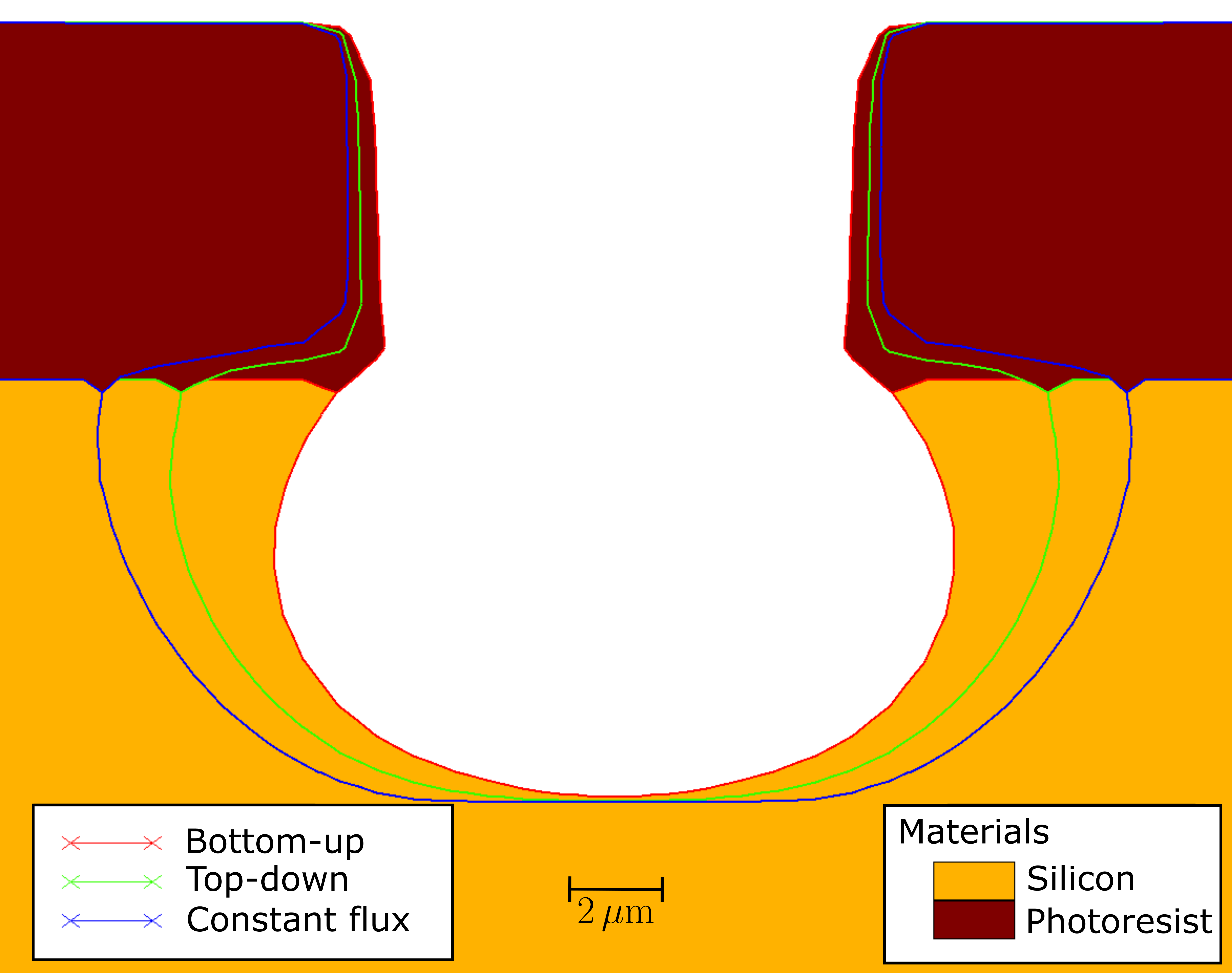
One key strength of topography simulations is that they enable the exploration of states which are not available experimentally. The state of the microcavity with initial \(d=\SI {12.4}{\micro \meter }\) is shown in Fig. 5.2 for the three proposed flux modeling approaches after the initial etch step but before photoresist removal. Although in principle available, this state was not experimentally
recorded due to resource constraints, as it would require electron microscopy. For the top-down simulation, the parameters from Tab. 5.2 are used, while for the bottom-up and
constant flux simulations the values of \(\mathit {PWR}_\mathrm {Si}\) are adjusted to yield the same microcavity depth. This highlights the success of the top-down approach and the limitations of the others. The bottom-up
approach is unable to capture the undercut which is a known experimental feature [171], leading to an unrealistically bulbous structure. Also, the perfectly flat bottom of the constant flux approach is again featured. Finally,
the simulations indicate the presence of photoresist tapering, which is a direction of interest for further process optimization.