As discussed in Section 5.4, the model parameters tend to be stable with respect to the reactor configuration. Therefore, the calibrated simulation can be used to investigate different
processing parameters in the same reactor configuration. That is, variations of the etch times can be computationally investigated without requiring further fabrication runs. In this section, the effect on the geometrical and optical
parameters of changing the first etch time, i.e., the etch time with photoresist present (\(t_\mathrm {resist}\)), as well as of varying the cumulative etch time (\(t_\mathrm {etch}\)), is investigated.
Firstly, it is fundamental to determine if the process inputs, i.e., the etch time, and the process outputs, i.e., the geometric quantities of interest, scale with a representative feature dimension. In this case, the representative scaling
dimension is the initial photoresist opening \(d\). This is crucial for further process optimization, since it addresses the issue of generalizability of the design guidelines to different feature scales. That is, if the resulting shape
follows a consistent scaling behavior, the optimized etch times can be applied to different photoresist configurations by considering the \(d\) scaling. Otherwise, other geometric scales such as, e.g., the photoresist thickness, might
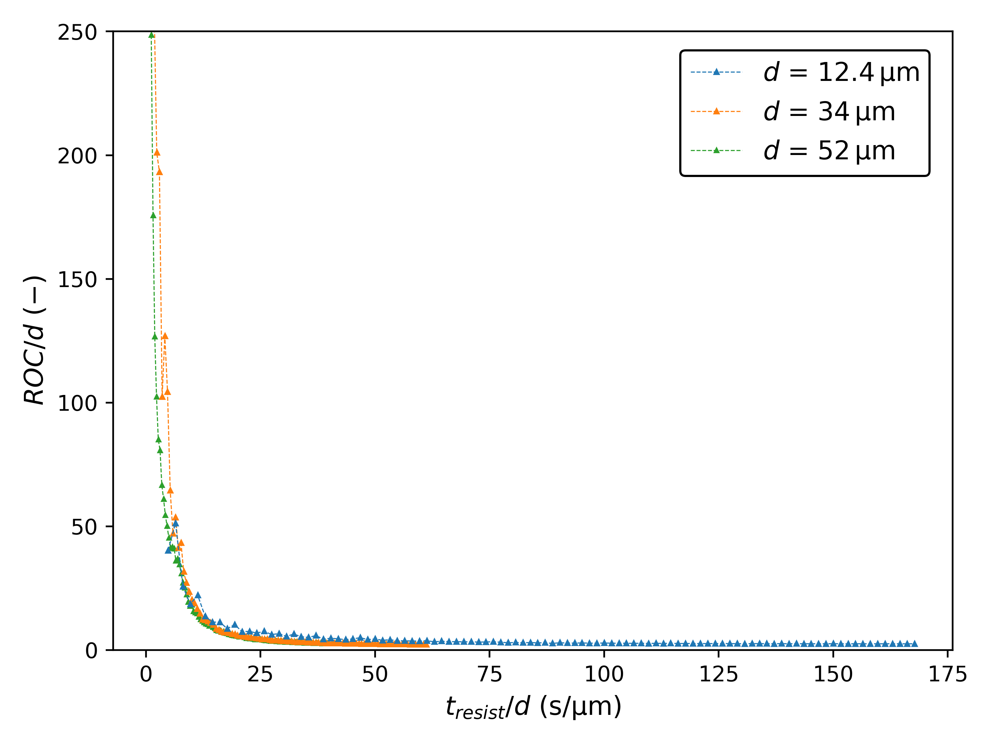
also play a role and should be considered. The determination of the scaling behavior is performed through a scale analysis, shown in Fig. 6.7. In it, both the main processing input,
the \(t_\mathrm {resist}\), and the key output, the ROC, are divided by the respective \(d\) for each of the three simulated cavities.
Figure 6.7 shows that the scaled evolutions of the ROC for the three studied cavities follow very similar curves which is evidence that \(d\) truly is the key physical scale.
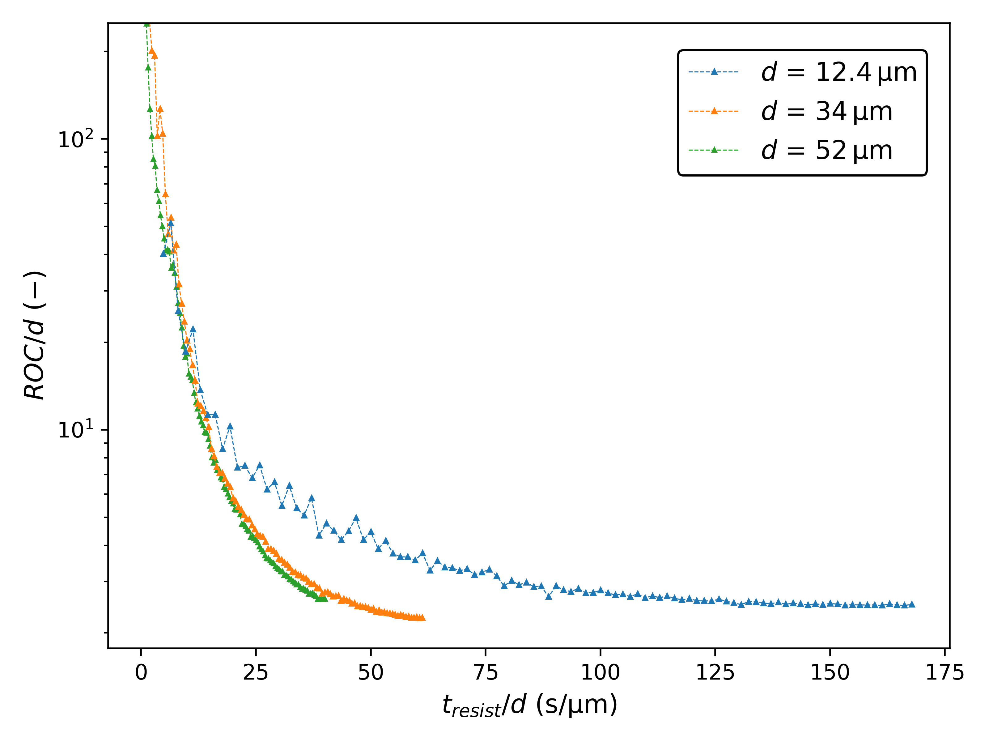
This enables further analyses to focus on a single cavity, since the results from the others can in principle be recovered via scaling. The same scaling behavior is plotted in Fig. 6.8 on
logarithmic axes. In this plot, the microcavities with \(d=\SI {34}{\micro \meter }\) and \(d=\SI {52}{\micro \meter }\) have a closer agreement than that with \(d=\SI {12.4}{\micro \meter }\). Although this is an
indication that other geometrical sizes, such as the photoresist thickness, could be affecting the smallest cavity, this should not be overemphasized. The logarithmic scale can exaggerate the effect of other phenomena, such as the
impact of the Monte Carlo noise or the intrinsic accuracy of the feature detection algorithm. Therefore, the conclusion that the process follows a single scaling behavior remains valid.
Figure 6.8: Scaling behavior of the ROC from Fig. 6.7 on logarithmic axes.
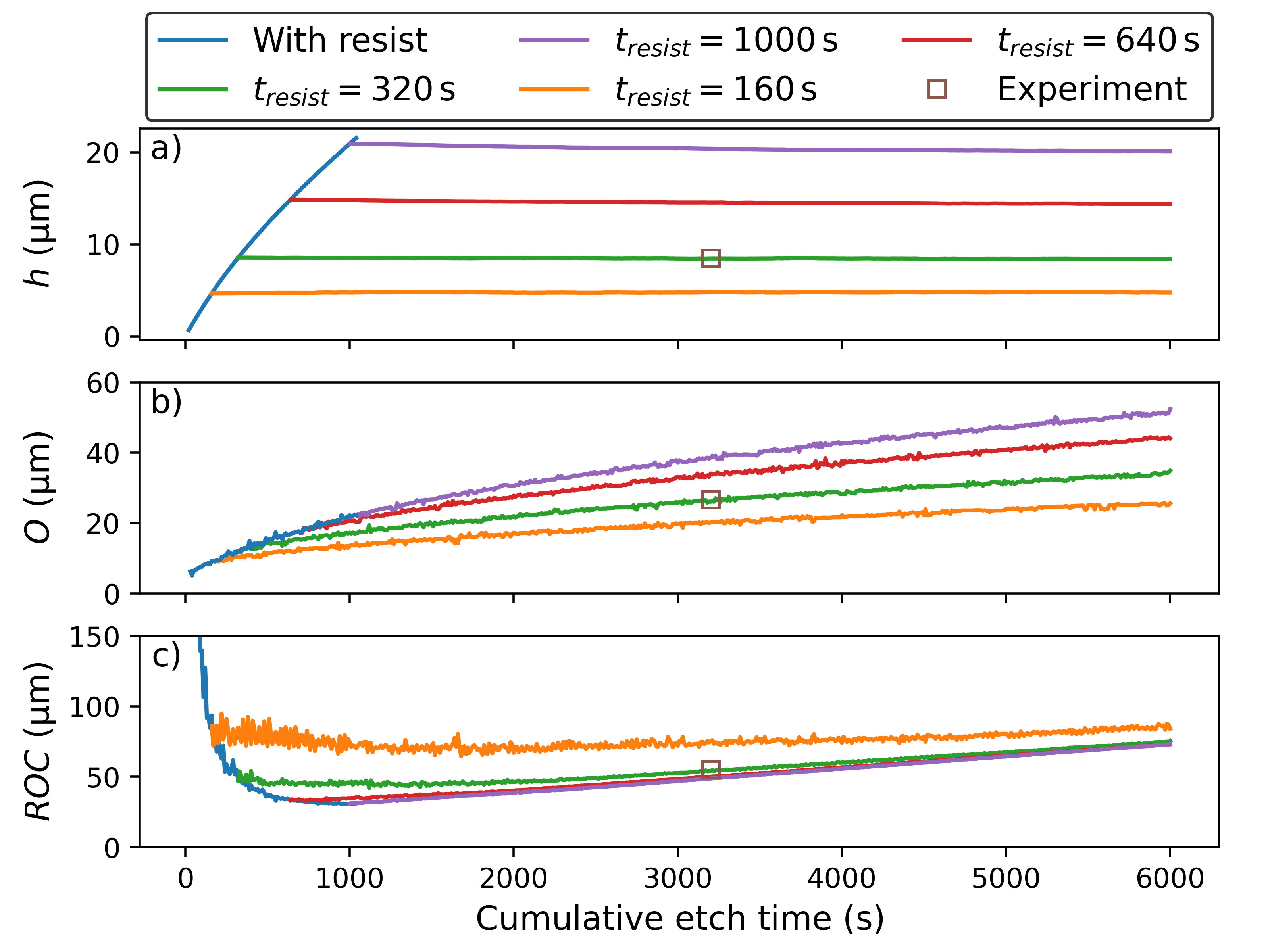
With the demonstrated scaling behavior of the characteristics of the microcavity, the time evolution of the geometric parameters \(h\), \(O\), and ROC can be investigated for a single microcavity with initial photoresist
opening \(d=\SI {12.4}{\micro \meter }\) for different simulated values of \(t_\mathrm {resist}\). This is depicted in Fig. 6.9 which also includes the same extracted
parameters from the experimental cavity etched with \(t_\mathrm {resist}=\SI {320}{\second }\) and \(t_\mathrm {etch}=\SI {3200}{\second }\), under the label "Experiment". Good agreement is shown between the
values extracted from simulated and experimental topographies which is a sign of the power of topography simulation in aiding the design process: If a similar analysis would be performed strictly experimentally, each point in the
plot would require a separate costly experiment. The noise in the extracted geometric parameters is a consequence of the top-down approach being a Monte Carlo method.
In Fig. 6.9.a), it can be remarked that the first etch step is directly responsible for determining the \(h\) of the cavity, as it remains stable during the second step. The
opening \(O\), however, shown in Fig. 6.9.b), is defined by both etch steps. Nonetheless, it can be noted that the rate of change of \(O\) is determined by the length of
\(t_\mathrm {resist}\). Finally, the ROC in Fig. 6.9.c) shows a competitive behavior between both etch steps. That is, the ROC has its lowest value
defined by the first etch step, reaching a minimum at \(t_\mathrm {resist}=\SI {1000}{\second }\), while the second etch step slowly increases it. According to the criteria in Eq. (6.6), the ROC should be kept to a minimum, thus, the second etch step should not be longer than necessary to reach the other optimization targets.
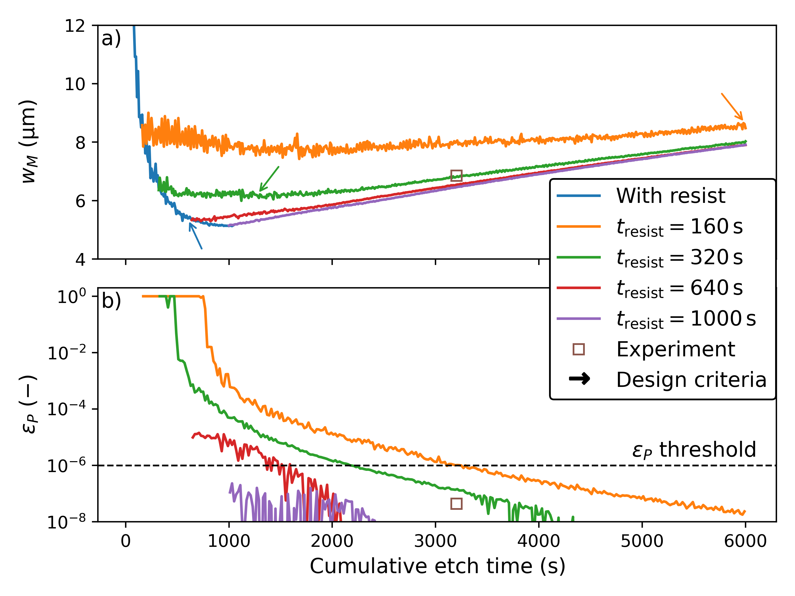
The remaining optimization design criteria from Eq. (6.6), namely those involving \(w_M\) and \(\epsilon _P\), can now be appreciated. The etch time
evolution of these optical parameters is shown in Fig. 6.10 for the same simulated microcavity with \(d=\SI {12.4}{\micro \meter }\). In Fig. 6.10.a), it can be seen that the \(t_\mathrm {etch}\) necessary to reach the design criterion \(O>6w_M\) is greatly reduced with increased \(t_\mathrm {resist}\). In fact, it
is already fulfilled during the first etch step at a time of approximately \(t_\mathrm {resist} = \SI {600}{\second }\). In combination with the observed reduction in ROC in Fig. 6.9.c), it appears that \(t_\mathrm {resist}\) should be increased by a factor of approximately \(2\) to improve microcavity quality. Attention must be placed, however, on
further processing issues which might arise such as loss of photoresist structural integrity [171] or photoresist hardening [185, 208].
So far, the discussion has focused on the effect of the first etch step. It is in observing Fig. 6.10.b) that the necessity of the second etch step becomes abundantly clear. Except
for the extreme values of \(t_\mathrm {resist}\), the quality of the cavity after the first step is very poor when analyzed through the lens of the parabolicity error from Eq. (6.5). As already motivated when this process was originally introduced [49], the second etch step is essentially isotropic, since there are no visibility effects from the
masking layer. This is crucial to converge the feature shape into a parabola. However, this realization exposes a trade-off when considered in conjunction with Fig. 6.9: The
second etch step is necessary to improve \(\epsilon _P\), however, it negatively impacts the ROC.
In conclusion, having achieved an accurate calibration to an experimentally manufactured cavity, the process could be efficiently explored via simulation. To improve the resonator quality, the first etch time should be increased as
much as possible, ideally by a factor of \(2\), while keeping in mind possibly arising issues such as photoresist instability. Although the second etch time is necessary in the context of reducing \(\epsilon _P\), it should not be
arbitrarily increased. As soon as \(\epsilon _P\) crosses below a specified threshold, the etching should be stopped such as to not negatively impact the ROC or increase costs. The analysis from Fig. 6.10 indicates that the second etch step can be reduced by up to \(50\,\%\), leading to a cumulative \(t_\mathrm {etch}\) reduction of \(35\,\%\) when also considering the
increase in \(t_\mathrm {resist}\). Finally, the scale analysis from Fig. 6.7 shows that there is room to further minimize the ROC by reducing the photoresist diameter
\(d\). However, this exploration should be performed carefully, since Fig. 6.8 indicates that a change of scaling regime could take place at excessively low values of \(d\).