The miniaturization of semiconductor devices has been a primary driver of the remarkable improvements in speed and performance of modern integrated circuits. Although devices fabricated at the 2 nm technology node have
already been demonstrated [1], transistor scaling shows clear signs of saturation as they approach physical and economic limits [2, 3, 4]. Additionally, gains in single-thread performance and clock frequency are severely limited, as
they come at the cost of unacceptably high active power consumption and heat dissipation. Due to the increased density of devices and leakage currents in integrated circuits, the stand-by power consumption is becoming a
significant concern as it approaches that of active operation [5], thus dramatically increasing the total power demand. In large-scale data centers, the high active power required for efficient data processing and memory data transfer
operations has accelerated in recent years due to the rapid growth in artificial intelligence, machine learning, and cryptocurrency applications [6]. The resulting power usage is increasingly unsustainable and directly at odds with the
global demand for reduced energy consumption. Consequently, new approaches are urgently needed to sustain technological progress while offering far more energy-efficient solutions.
One promising strategy for reducing energy consumption is to introduce non-volatility into both main and cache memory, thereby eliminating the stand-by power [7, 3]. Furthermore, embedding non-volatile memory close to, or
directly on, the processor would further minimize long interconnects and energy-intensive data transfers. Beyond lowering stand-by power, such integration also paves the way for in-memory computing, a paradigm that combines
low energy consumption with high performance [8, 3]. Among emerging non-volatile memory technologies, magnetoresistive random-access memory (MRAM) is particularly promising. Magnetic tunneling junctions (MTJs), the
building blocks of MRAM where the bit value is stored in the relative magnetization direction of two ferromagnetic (FM) layers separated by an insulating layer, offer complementary metal oxide semiconductor (CMOS)
compatibility, a simple device structure, long data retention, high endurance, fast switching, and scalability [9].
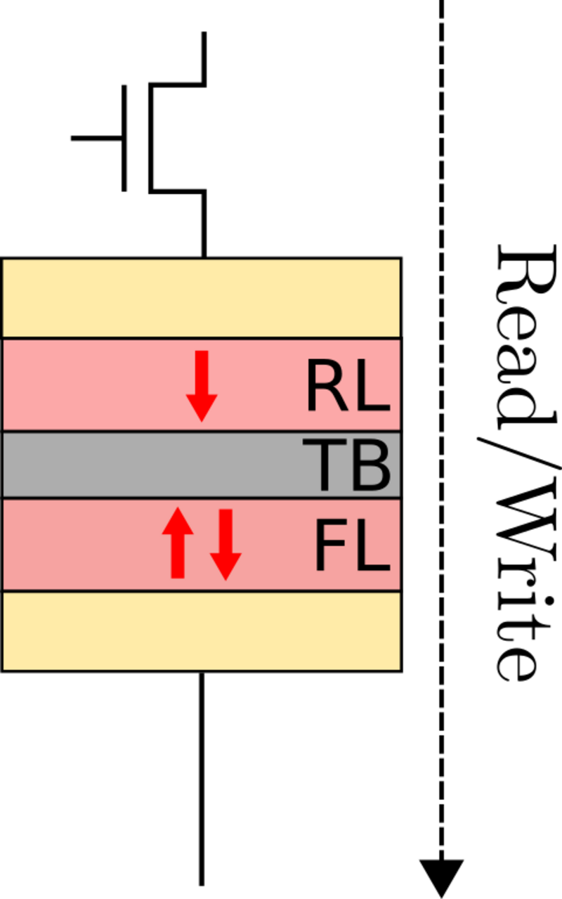
(a) STT-MRAM cell
(b) SOT-MRAM cell
Figure 1.1: Schematics of the typical STT- and SOT-MRAM cell structures. The main component of both structures is the MTJ, which stores the bit value in the relative magnetization orientation (red arrows) of two FM
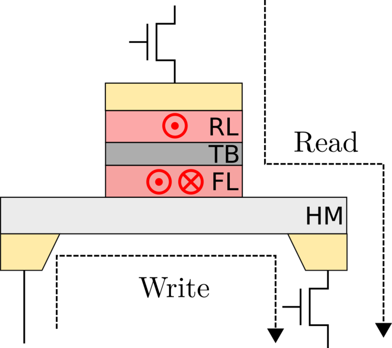
layers, which can be either parallel or anti-parallel. In STT-MRAM, the write path goes through the MTJ, while in SOT-MRAM, the write path goes through a SOT layer beneath the MTJ.
Modern MRAM can be split into two main categories: spin-transfer torque MRAM (STT-MRAM) and spin-orbit torque MRAM (SOT-MRAM) [9]. The key difference lies in the mechanism used to switch the logical state of the
MTJs, which affects their performance and scalability. The typical cell structures of STT- and SOT-MRAM are illustrated in Fig. 1.1. STT-MRAM is highly scalable;
however, the switching speed and endurance of the cell are limited due to the shared read and write path. In contrast, SOT-MRAM has separate read and write paths, achieved by leveraging nonmagnetic (NM) materials with
strong spin-orbit coupling (SOC), which enables faster switching speeds, lower power consumption, and improved endurance at the cost of reduced scalability. STT-MRAM is a mature technology with commercial products already
available and sold by several companies with densities up to 1 GB [10]. SOT-MRAM, on the other hand, is still in an early research and development phase but holds significant promise for future applications, especially in
cache memory, where speed and endurance are more critical than density [11].
Until now, MRAM has only been a niche technology mainly used in specific automotive, aerospace, mobile, and data center applications. For MRAM to become a widely adopted technology, the success of its deployment in main
memory and cache is essential. However, the advantages of non-volatility are currently offset by the high switching currents and large write energies required, as well as the challenges of difficult deterministic switching, low density,
and back-end of line (BEOL) integration [11]. Several promising approaches are under investigation to address these challenges, including novel energy-efficient materials, voltage-controlled magnetic anisotropy (VCMA) switching,
multi-bit cells, and antiferromagnetic (AFM) MTJs [11].
Historically, the success of microelectronics has relied heavily on sophisticated technology computer-aided design (TCAD) tools [12]. However, accurate TCAD support for MRAM is still largely lacking, which poses a significant
barrier to its widespread adoption. The goal of the research presented in this work was to address this gap by developing advanced modeling and simulation methods and tools tailored to SOT-MRAM. Ultimately, enabling
comprehensive, three-dimensional (3D) simulations of spin currents, spin torques, and magnetization dynamics in advanced SOT-MRAM device structures.
1.1 Outline of the Thesis
This thesis focuses on the development and application of simulation tools designed to model the SOTs present in FM systems with strong SOC, aiming to simulate SOT-driven magnetization dynamics accurately. The results
presented herein were generated with the described models and methods, which were implemented using software built on C++ and Python libraries. The thesis is structured as follows:
• Chapter 2 gives an overview of some fundamental concepts and phenomena in spintronics that are relevant to the research
presented in this dissertation.
• Chapter 3 presents the micromagnetic model used to describe the magnetization dynamics in FM materials and the effective
field contributions considered.
• Chapter 4, the spin and charge transport model employed to calculate the SOTs in multilayer structures is described in
detail, along with the boundary conditions (BCs).
• Chapter 5 presents the derivation of two different sets of BCs used for modeling interfacial SOC: one based on a
perturbative treatment of the Rashba SOC at NM/FM interfaces, and a non-perturbative direct treatment based on an effective interface field approach.
• Chapter 6, the numerical methods and implementations used to solve the micromagnetic and spin and charge
transport equations are presented in detail, along with the quadrature scheme used for the Fermi surface integrals.
• Chapter 7, the SOTs arising from bulk and interfacial SOC in NM/FM bilayers and FM/NM/FM
trilayers are studied and analyzed using the numerical methods.
• Chapter 8, the developed simulation tools are applied to study SOT-driven magnetization
dynamics during switching in various SOT-MRAM devices.
• Chapter 9, summarizes the main results of this thesis and discusses possible directions for future research.
• Appendix A contains the analytical expressions for the interface conductances obtained from considering an interfacial
exchange interaction delta-function potential.
• Appendix B presents the one-dimensional (1D) analytical solution of the transport model for a NM/FM
bilayer.