

Modeling Spin-Orbit Torques
in Advanced Magnetoresistive Devices
6.4 Weak Formulation of the Drift-Diffusion
Equations
In this section, the weak formulation and implementation of the 3D charge and spin drift-diffusion equations and the various BCs considered are presented. Furthermore, the accuracy of the implementation is tested and validated for a quasi-1D system. Since the final goal is to compute the torques acting on the magnetization, computing the effects of the spin on the electrical current is not necessary. Therefore, to simplify the computation, the charge and spin PDEs are solved separately by using the decoupled PDEs from Chapter 4, Section 4.4.2. The effects of the spin on the electrical current can be included using the iterative approach if necessary.
6.4.1 Electrical Potential
A multilayer system \(\Omega \) with FM regions \(\omega \subset \Omega \) is considered. To compute the charge current density \(\bm {j_c}\) and the electrical potential \(V_c\) in \(\Omega \) the following problem has to be solved:
\(\seteqnumber{1}{6.50}{0}\)\begin{align} \nabla \cdot \bm {j_c} & = 0 & & \text {in } \Omega , \\ \bm {j_c}\cdot \bm {n} & = 0 & & \text {on } \partial \Omega \setminus \Gamma ^i, \\ V_c & = V_c^i & & \text {on } \Gamma ^i, \end{align} where \(V_c^i\) is the Dirichlet BC for the electrical potential \(V_c\) on the contact \(\Gamma ^i\), which translates to the applied voltage. For now, the internal boundaries are disregarded. Integrating the first equation over the domain \(\Omega \) and performing the integration by parts gives
\(\seteqnumber{0}{6.}{50}\)\begin{equation} \langle \nabla \cdot \bm {j_c}, w \rangle _\Omega = \langle \bm {n}\cdot \bm {j_c},w\rangle _{\partial \Omega } - \langle \bm {j_c},\nabla w\rangle _\Omega = 0, \end{equation}
where the compact notation \(\langle f,g \rangle _\Omega = \int _{\Omega } fg d\bm {r}\), and \(\langle \bm {f},\bm {g} \rangle _\Omega = \int _{\Omega } \bm {f}\cdot \bm {g} d\bm {r}\), is used. Inserting the expression for the current density \(\bm {j_c} \) and collecting the terms without \(V_c\) on the right-hand side yields the weak formulation of the electrical potential and current density: find \(V_c \in H^1(\Omega )\) such that
\(\seteqnumber{0}{6.}{51}\)\begin{equation} \sigma \langle \nabla V_c, \nabla w \rangle _\Omega = \frac {e}{\mu _B}\beta _{D}D_e \langle (\nabla \bm {S^\prime })^T\bm {m},\nabla w\rangle _\Omega + \frac {e}{\mu _B}\alpha _\mathrm {SHA}D_e\langle \nabla \times \bm {S^\prime },\nabla w\rangle _\Omega , \,\forall \, w \in H^1(\Omega ). \end{equation}
The vector space for the test function is chosen to be \(H^1(\Omega ) \coloneqq \{v\in L^2(\Omega ): v^\prime \in L^2(\Omega )\}\), referred to as the first-order Sobolev space. Simply put, \(H^1(\Omega )\) is the space of functions where the functions and their first order derivatives belong to the space of square integrable functions \(L^2(\Omega )\). The electrical current density is then computed from the solution for the electrical potential and the previous solution of the spin accumulation:
\(\seteqnumber{0}{6.}{52}\)\begin{equation} \bm {j_c} = -\sigma \nabla V_c + \frac {e}{\mu _B}\beta _{D}D_e(\nabla \bm {S^\prime })^T\bm {m} + \frac {e}{\mu _B}\alpha _\mathrm {SHA}D_e\nabla \times \bm {S^\prime }. \end{equation}
6.4.2 Spin Accumulation
To compute the spin accumulation \(\bm {S}\) the following problem has to be solved on the domain \(\Omega \):
\(\seteqnumber{1}{6.54}{0}\)\begin{align} \nabla \tilde {J}_s & = -D_e\left ({\frac {\bm {S}}{\lambda _{sf}^2} + \frac {\bm {S}\times \bm {m}}{\lambda _J^2} +\frac {\bm {m}\times (\bm {S}\times \bm {m})}{\lambda _\phi ^2}}\right ) \quad & & \text {in } \Omega , \\ \tilde {J}_s\bm {n} & = 0 \quad & & \text {on } \partial \Omega \setminus \Gamma _i, \\ \tilde {J}_s\bm {n} & = - \frac {D_e}{\lambda _{sf} }\bm {S} \quad & & \text {on } \Gamma _i. \end{align} For now, the internal boundaries are neglected. Multiplying the equation by a test function \(\bm {\zeta } \in \bm {H^1}(\Omega )\), integrating over the domain, and using integration by parts gives
\(\seteqnumber{0}{6.}{54}\)\begin{equation} \langle \nabla \tilde {J}_s, \bm {\zeta } \rangle _{\Omega } = \langle \tilde {J}_s\bm {n}, \bm {\zeta } \rangle _{\partial \Omega } -\langle \tilde {J}_s, \nabla \bm {\zeta } \rangle _{\Omega } = -\frac {D_e}{\lambda _{sf}^2}\langle \bm {S},\bm {\zeta }\rangle _\Omega -\frac {D_e}{\lambda _{J}^2}\langle \bm {S}\times \bm {m},\bm {\zeta }\rangle _\omega -\frac {D_e}{\lambda _{\phi }^2}\langle \bm {m}\times (\bm {S}\times \bm {m}),\bm {\zeta }\rangle _\omega . \end{equation}
The vector space \(\bm {H^1}(\Omega )\) is defined as the space of vector functions where each component of the functions belongs to the first-order Sobolev space \(H_1(\Omega )\).
Inserting the expression for the spin current density \(\tilde {J}_s\) (Eq. (4.44)) in the bulk term, the Neumann and Robin conditions for the spin current in the boundary term, and collecting the terms containing \(\bm {S}\) on the left-hand side yields the weak formulation of the spin accumulation: find \(\bm {S} \in \bm {H^1}(\Omega )\) such that
\(\seteqnumber{0}{6.}{55}\)\begin{multline} \label {eq:weak_form_spin_accumulation} D_e\langle \nabla \bm {S},\nabla \bm {\zeta }\rangle _\Omega - \beta _\sigma \beta _D D_e\langle \bm {m}\otimes [(\nabla \bm {S})^T\bm {m}],\nabla \bm {\zeta }\rangle _\omega -\alpha _\mathrm {SH}D_e\langle \nabla \times \bm {S},\nabla \times \bm {\zeta }\rangle _{\Omega } -\frac {D_e}{\lambda _{sf}}\langle \bm {S},\bm {\zeta }\rangle _{\Gamma _i}+\frac {D_e}{\lambda _{sf}^2}\langle \bm {S},\bm {\zeta }\rangle _\Omega +\frac {D_e}{\lambda _{J}^2}\langle \bm {S}\times \bm {m},\bm {\zeta }\rangle _\omega +\frac {D_e}{\lambda _{\phi }^2}\langle \bm {m}\times (\bm {S}\times \bm {m}),\bm {\zeta }\rangle _\omega \\ = -\frac {\mu _B}{e}\beta _\sigma \langle \bm {m}\otimes \bm {j_c},\nabla \bm {\zeta } \rangle _\omega -\frac {\mu _B}{e}\alpha _\mathrm {SHA}\langle \varepsilon \bm {j_c},\nabla \bm {\zeta } \rangle _\Omega \qquad \forall \, \bm {\zeta } \in \bm {H^1}(\Omega ). \end{multline} Here the volume integral \(\langle \nabla \bm {f},\nabla \bm {g} \rangle _\Omega = \int _\Omega \nabla \bm {f}:\nabla \bm {g} \, d\bm {r}\) was introduced, where \(A:B = \sum _{ij} A_{ij}B_{ij}\) is the Frobenius product.
6.4.3 Magnetic Tunneling Junctions
The TB is included in the weak formulation for the electrical potential, and is modeled as a poor conductor with a low conductivity, which depends on the local relative magnetization direction of the two adjacent FM layers. The conductivity in the TB is given by
\(\seteqnumber{0}{6.}{56}\)\begin{equation} \sigma (\bm {r}) = \sigma _0\left [1 + P_{1}P_{2}\bm {m_1}(\bm {r})\cdot \bm {m_2}(\bm {r})\right ], \end{equation}
where \(\sigma _0 = \mathcal {G}_0 d_\mathrm {TB}/A \) is the conductivity of the TB with thickness \(d_\mathrm {TB}\) and surface area \(A\). The vector \(\bm {m_{1/2}}(\bm {r}) = \bm {m}(P_{1/2}(\bm {r}))\) is the magnetization located at the interface \(\Gamma _{1/2}\), where \(P_{1/2}\) maps points inside the TB to the nearest point on interface \(\Gamma _{1/2}\). The contribution to the weak formulation for the electrical potential in the TB thus reads
\(\seteqnumber{0}{6.}{57}\)\begin{equation} \sigma _0\langle \left (1 + P_{1}P_{2}\bm {m_1}\cdot \bm {m_2}\right ) \nabla V_c, \nabla w \rangle _{\Omega _\mathrm {TB}} = 0, \end{equation}
where the position dependence was omitted for brevity.
Tunneling spin current density \(\tilde {J}^\mathrm {TB}_s\bm {n}\) can be directly applied as Neumann BCs at the interfaces of the TB \(\Gamma _{1/2}\). The magnetization at a given position on one interface is mapped to the nearest point on the other interface through an isomorphism \(P_{12}:\Gamma _1\to \Gamma _2\). The contribution to the weak formulation for the spin accumulation in the TB is added to the linear form, and reads
\(\seteqnumber{0}{6.}{58}\)\begin{equation} l_\mathrm {TB} (\bm {\zeta }) = \langle \tilde {J}^\mathrm {TB}_s\bm {n},\bm {\zeta }\rangle _{\Gamma _1} + \langle \tilde {J}^\mathrm {TB}_s\bm {n},\bm {\zeta }\rangle _{\Gamma _2}. \end{equation}
6.4.4 Magnetoelectronic Circuit Theory Boundary
Conditions
The spin current BCs from the MCT can be expressed as
\(\seteqnumber{1}{6.60}{0}\)\begin{align} \bm {j_c}\cdot \bm {n} & = G_{cc} \Delta \bm {V_c} + \bm {G_{sc}}\cdot \Delta \bm {V^\prime _s}, \\ \bm {J_s}\bm {n} & = \frac {\mu _B}{e}(\tilde {G}_{ss} - \bm {G_{sc}}\otimes \bm {G_{sc}}G^{-1}_{cc})\Delta \bm {V_s} + \frac {\mu _B}{e}\bm {G_{sc}}G^{-1}_{cc} (\bm {j_c}\cdot \bm {n}), \end{align} where \(G_{cc} = G_{\uparrow \uparrow } - G_{\downarrow \downarrow }\) is the charge conductance, \(\bm {G_{sc}} = (G_{\uparrow \downarrow } - G_{\downarrow \uparrow })\bm {m}\) is the spin-charge conductance vector, and \(\tilde {G}_{ss} = (G_{\uparrow \downarrow } + G_{\downarrow \uparrow })\bm {m}\otimes \bm {m} -2\operatorname {Re}\{G_{\uparrow \downarrow }\}[\bm {m}]_\times [\bm {m}]_\times + 2\operatorname {Im}\{G_{\downarrow \downarrow }\}[\bm {m}]_\times \) is the spin conductance tensor. Following the steps in Section 6.3.3, the weak formulation of the BCs reads
\(\seteqnumber{0}{6.}{60}\)\begin{equation} -G_{cc}\langle \Delta \bm {V_c}, \Delta w\rangle _\Gamma = \langle \bm {G_{sc}}\cdot \Delta \bm {V^\prime _s},\Delta w \rangle _{\Gamma }, \end{equation}
for the electrical potential, and
\(\seteqnumber{0}{6.}{61}\)\begin{equation} -\frac {\mu _B}{e}\langle (\tilde {G}_{ss} - \bm {G_{sc}}\cdot \bm {G_{sc}}G^{-1}_{cc})\Delta \bm {V_s}, \Delta \bm {\zeta }\rangle _\Gamma = \frac {\mu _B}{e}G^{-1}_{cc}\langle \bm {G_{sc}}(\bm {j_c}\cdot \bm {n}), \Delta \bm {\zeta }\rangle _\Gamma , \end{equation}
for the spin accumulation, on the NM/FM boundary \(\Gamma \). The conductances that depend on the magnetization must be included in the integral, as the magnetization can vary across the interface. Using the effective interface layer approximation, one obtains
\(\seteqnumber{0}{6.}{62}\)\begin{equation} -d_{eff} G_{cc}\langle (\bm {n}\cdot \nabla )V_c, (\bm {n}\cdot \nabla ) w\rangle _{\Omega _{eff} } = d_{eff}\langle \bm {G_{sc}}\cdot [(\bm {n}\cdot \nabla )\bm {V^\prime _s}],(\bm {n}\cdot \nabla )w \rangle _{\Omega _{eff} }, \end{equation}
and
\(\seteqnumber{0}{6.}{63}\)\begin{equation} -d_{eff} \frac {\mu _B}{e}\langle (\tilde {G}_{ss} - \bm {G_{sc}}\cdot \bm {G_{sc}}G^{-1}_{cc})[(\bm {n}\cdot \nabla )\bm {V_s}], (\bm {n}\cdot \nabla )\bm {\zeta }\rangle _{\Omega _{eff} } = \frac {\mu _B}{e} G^{-1}_{cc}\langle \bm {G_{sc}}(\bm {j_c}\cdot \bm {n}), (\bm {n}\cdot \nabla )\bm {\zeta }\rangle _{\Omega _{eff}}, \end{equation}
which is included in the weak formulation for the electrical potential and spin accumulation, respectively. The magnetization is accessed in the effective interface layer through the mapping \(\bm {m}(P_{i}(\bm {r}))\) as in the TB case, where \(i \in \{1,2\}\) depends on which side of the interface is the FM layer.
6.4.5 Interfacial Spin-Orbit Coupling Boundary
Conditions
Using the BCs derived in chapter 5 for the interfacial SOC, the weak formulation of the BCs reads
\(\seteqnumber{0}{6.}{64}\)\begin{equation} -\langle G_{cc} \Delta \bm {V_c}, \Delta w\rangle _\Gamma = \langle \bm {G_{sc}}\cdot \Delta \bm {V^\prime _s}, \Delta w \rangle _{\Gamma } + \langle j_c^R,\Delta w\rangle _\Gamma , \end{equation}
for the electrical potential, where \(j_c^R\) is the Rashba charge current density at the interface, and
\(\seteqnumber{0}{6.}{65}\)\begin{equation} -\frac {\mu _B}{e}\langle (\tilde {G}_{ss} - \bm {G_{sc}}\cdot \bm {G_{sc}}G^{-1}_{cc}) \Delta \bm {V_s}, \Delta \bm {\zeta }\rangle _\Gamma -\frac {\mu _B}{e}\langle \Delta \tilde {G}_{ss} \bm {\overline {V_s}},\bm {\overline {\zeta }}\rangle _\Gamma = \frac {\mu _B}{e}\langle \bm {G_{sc}}G^{-1}_{cc}(\bm {j_c}\cdot \bm {n}), \Delta \bm {\zeta }\rangle _\Gamma + \langle \Delta \bm {J_s^R},\bm {\overline {\xi }}\rangle _\Gamma + \langle \bm {\overline {J}_s^R},\Delta \bm {\xi }\rangle _\Gamma , \end{equation}
for the spin accumulation, where \(\bm {J_s^R}\) and \(\bm {\Delta J_s^R}\) are the average and difference of Rashba spin current densities across the interface, respectively. They are obtained from taking the average and difference across the interface of the spin conductivity terms. Here \(\tilde {G}_{ss}\) is an average spin conductance tensor, while \(\Delta \tilde {G}_{ss}\) is a spin conductance tensor difference across the interface. These are determined by taking the average and difference of the spin current densities across the interface. For the effective interface field BCs: \(G_{cc} = G_+\), \(\bm {G_{sc}} = \bm {G_-}\), \(\tilde {G}_{ss} = \tilde {G}_+ - (\tilde {G}_{\uparrow \downarrow } + \tilde {\Gamma }_{\uparrow \downarrow })\), and \(\Delta \tilde {G}_{ss} = \tilde {G}_{\uparrow \downarrow } - \tilde {\Gamma }_{\uparrow \downarrow }\). For the perturbation theory approach, where the MCT conductances are used instead, \(\Delta \tilde {G}_{ss} = 0\), while the other conductances are the same as in the previous section.
Using the effective interface layer approximation, the contribution to the weak formulation reads
\(\seteqnumber{0}{6.}{66}\)\begin{equation} -d_{eff} \langle G_{cc}(\bm {n}\cdot \nabla )V_c, (\bm {n}\cdot \nabla ) w\rangle _{\Omega _{eff} } = d_{eff}\langle \bm {G_{sc}}\cdot [(\bm {n}\cdot \nabla )\bm {V^\prime _s}], (\bm {n}\cdot \nabla )w \rangle _{\Omega _{eff} } + \langle j_c^R,(\bm {n}\cdot \nabla )w\rangle _{\Omega _{eff}}, \end{equation}
and
\(\seteqnumber{0}{6.}{67}\)\begin{multline} -d_{eff}\frac {\mu _B}{e}\langle (\tilde {G}_{ss} - \bm {G_{sc}}\cdot \bm {G_{sc}}G^{-1}_{cc})[(\bm {n}\cdot \nabla )\bm {V_s}], (\bm {n}\cdot \nabla )\bm {\zeta }\rangle _{\Omega _{eff}} - \frac {\mu _B}{e} d^{-1}_{eff}\langle \Delta \tilde {G}_{ss}\bm {V_s},\bm {\zeta }\rangle _{\Omega _{eff}} \\ = \frac {\mu _B}{e}\langle \bm {G_{sc}}G^{-1}_{cc} (\bm {j_c}\cdot \bm {n}), (\bm {n}\cdot \nabla )\bm {\zeta }\rangle _{\Omega _{eff}} + d^{-1}_{eff}\langle \Delta \bm {J_s^R},\bm {\xi }\rangle _{\Omega _{eff}} + \langle \bm {\overline {J}_s^R},(\bm {n}\cdot \nabla )\bm {\xi }\rangle _{\Omega _{eff}}, \end{multline} for the electrical potential and spin accumulation, respectively.
6.4.6 FEM Implementation
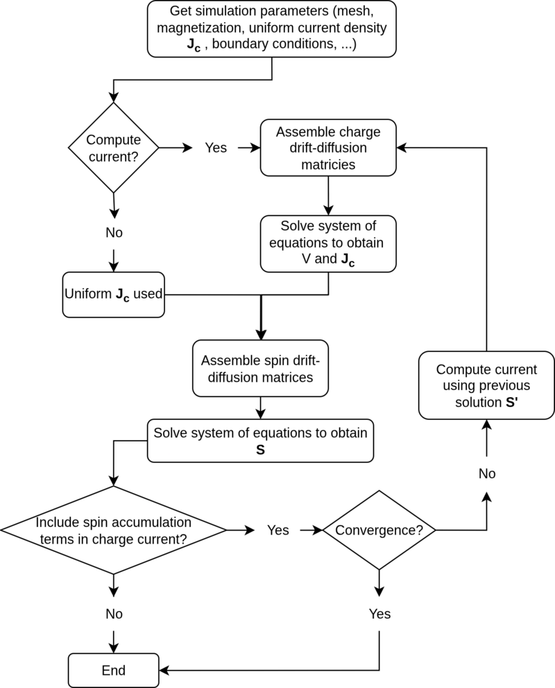
The charge and spin drift-diffusion equations are solved by the in-house simulation software ViennaSpinMag [86], an open-source FEM-based tool for numerical investigation of MRAM devices. The software is modular and contains modules for the charge drift-diffusion, spin drift-diffusion, and the LLG equation, which can be used independently or in combination. For this work, the charge and spin drift-diffusion modules of the software have been extended to include the SHE and ISHE, the MCT BCs, as well as the interfacial SOC BCs from the previous chapter. The software is written in \(C_{++}\) and uses the open-source FEM framework MFEM [87] to assemble and solve the weak formulation of the drift-diffusion equations for a given mesh. The resulting linear system of equations for the electrical potential is solved using the conjugate gradient (CG) method, while the spin accumulation system is solved using the generalized minimal residual (GMRES) method, provided by the MFEM library. The CG method is an iterative algorithm for solving matrix equations where the matrix is positive-definite, as is the case of the weak formulation for the electrical potential. The GMRES method is an iterative method used for solving indefinite non-symmetric linear systems, which due to the cross product terms makes it suitable for solving the weak formulation for the spin accumulation.
The spin accumulation can be computed using a uniform current density or by computing the electrical potential for the given mesh and then computing the current density from the gradient of the electrical potential. A flow chart of the charge and spin drift-diffusion implementation is shown in Fig. 6.8. To include the spin accumulation terms in the current computation, such as the ISHE term, the iterative approach is used, where the current is first computed without these terms, then the spin accumulation is computed using the current from the previous iteration, and finally, the current is computed again using the spin accumulation. This process is repeated until the solution for the spin accumulation converges, i.e., the change in the spin accumulation between two iterations is below a given threshold \(\epsilon \):
\(\seteqnumber{0}{6.}{68}\)\begin{equation} \frac {\lVert \bm {S^n} \rVert _{L^2} - \lVert \bm {S^{n-1}} \rVert _{L^2}}{\lVert \bm {S^n} \rVert _{L^2}} < \epsilon , \end{equation}
where \(\lVert \bm {S_n} \rVert _{L^2}\) is the \(L^2\) norm of the spin accumulation at iteration \(n\).
In the next subsection, the accuracy and the validity of the SHE and effective interface layer BC implementations are assessed through numerical tests. The meshes used in the tests and in the rest of this work are generated using the open-source mesh generator NetGen [88].
6.4.7 One-Dimensional Bilayer System Test
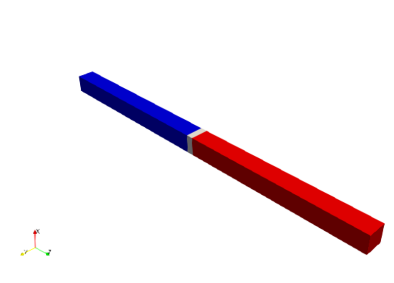
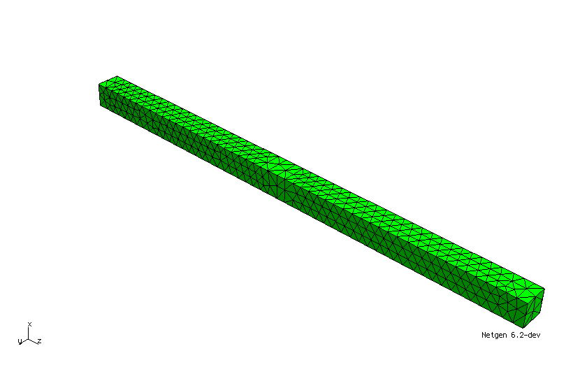
To validate the effective interface layer approximation, the CIP NM/FM bilayer system from Section 6.2.4 is again considered. To compare directly with the analytical solution, the 3D weak formulation must be reduced to one dimension. This is achieved by limiting the spin polarization and spin Hall spin currents in the linear form to the \(z\)-direction, i.e., \(\bm {m}\otimes \bm {j_c} \to 0\) and \(\varepsilon \bm {j_c} \to \bm {\hat {y}}\otimes \bm {\hat {z}}j_{cx}\) for a current along the \(x\)-axis in the left-hand-side of Eq. (6.56). Furthermore, a quasi-1D mesh of the bilayer system is used, as shown in Fig. 6.9.
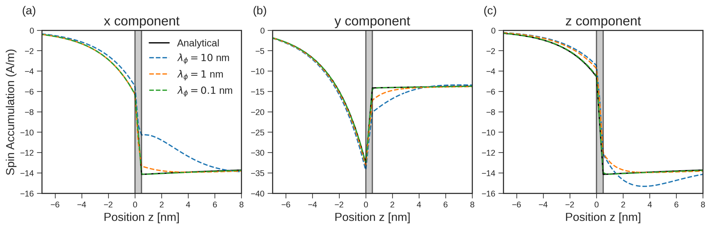
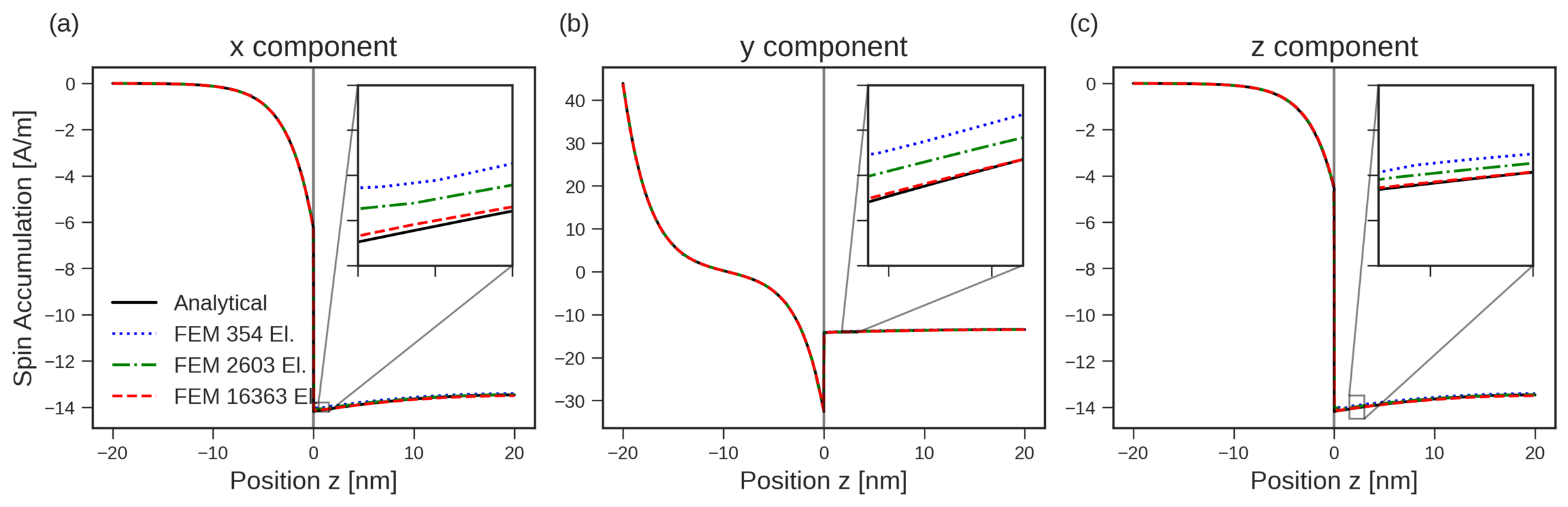
Figure 6.10 shows the comparison of the quasi-1D FEM and analytical solutions for the spin accumulation in a NM(20 nm)/FM(20 nm) bilayer system for a varying spin dephasing length \(\lambda _\phi \). As the analytical solution was obtained by assuming that the transverse spin is instantly absorbed in the FM layer, the FEM solution converges to the analytical solution for \(\lambda _\phi \to 0\). For \(\lambda _\phi = 0.1\,\mathrm {nm}\), the FEM solution is in good agreement with the analytical solution, while for \(\lambda _\phi = 10\,\mathrm {nm}\), the FEM solution deviates significantly from the analytical solution in the FM layer.
Figure 6.11 shows the comparison of the FEM and analytical solutions for the spin accumulation in a NM(20 nm)/FM(20 nm) bilayer system with a fixed spin dephasing length \(\phi = 0.1\) nm and an increasingly refined mesh. The effective interface layer is subtracted from the presented solution. The FEM solution shows good agreement for all the meshes. By zooming in on the solution, it can be seen that the FEM solution converges to the analytical solution as the mesh is increasingly refined.
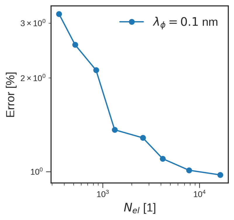
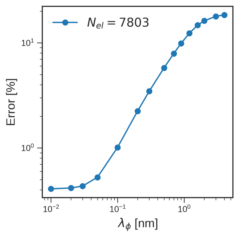
Figure 6.12 shows the NMAE between the FEM and analytical solutions as a function of the number of elements for a fixed spin dephasing length of \(\lambda _\phi = 0.1\,\mathrm {nm}\), and as a function of the spin dephasing length for a fixed number of elements \(N_\mathrm {el} = 2603\). Both figures show that a good convergence of the FEM solution to the analytical solution is achieved when the number of elements is increased or when the spin dephasing length is decreased.