To eliminate the need for an external magnetic field, several field-free switching (FFS) schemes have been proposed. One of the earliest and simplest FFS schemes proposed is to combine SOTs with STTs by adding a current pulse
through the MTJ in addition to the current pulse through the NM layer. This approach was first studied in the mid-2010s by evaluating the LLG equation [146, 147], and later demonstrated experimentally in 2018 by Wang et
al. [148]. The switching is achieved through two phases: first, a timed current pulse is applied through the NM layer to eliminate the incubation time by bringing the magnetization in-plane with SOTs, followed by a current
pulse through the MTJ, which completes the switching through STTs. The timing and magnitude of the two current pulses can vary depending on the desired device characteristics, as they can be optimized for speed, energy
efficiency, endurance, and reliability. This section explores the switching of a FL with PMA using the combined interplay of SOTs and STTs.
(a) Device
(b) Mesh
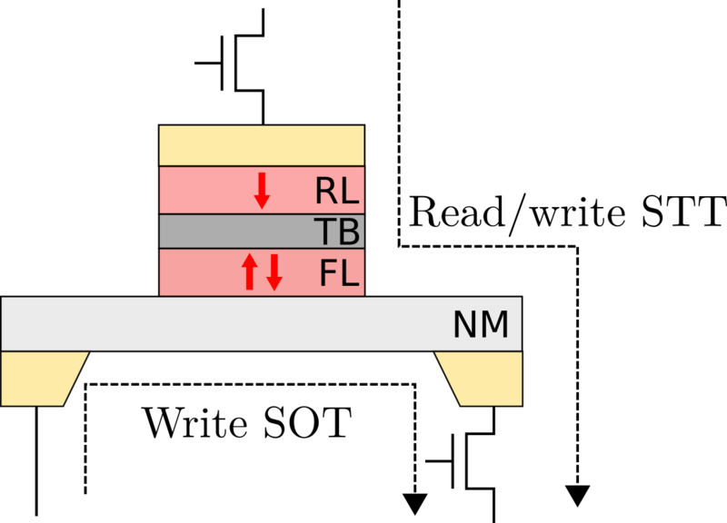
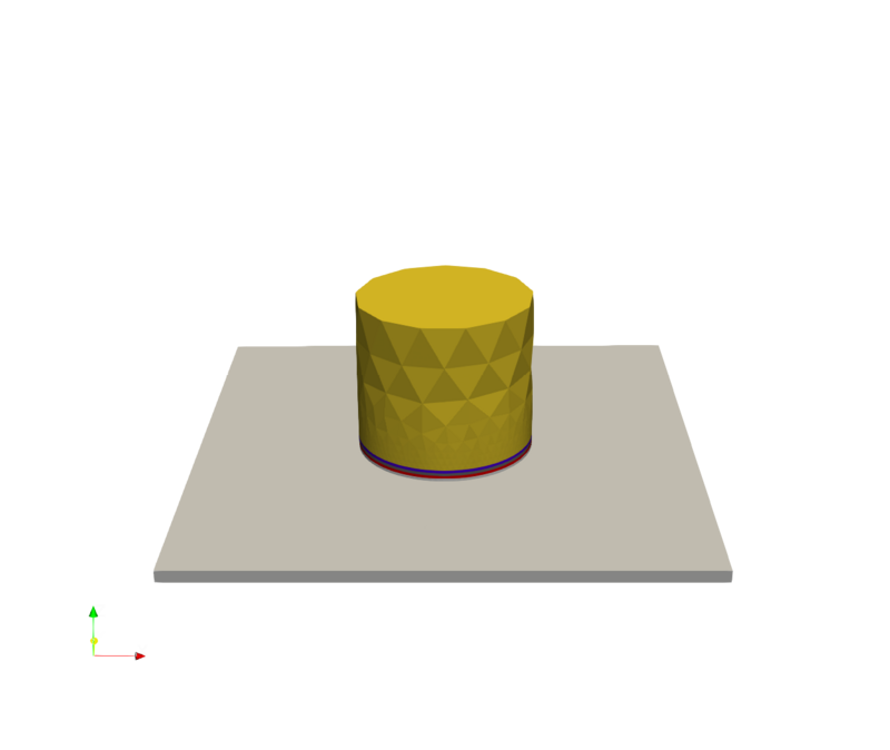
Figure 8.7: Schematic of a hybrid STT-SOT-MRAM device with PMA (a), and the corresponding mesh used for the simulations (b). Red arrows indicate the magnetization direction of the FL and RL. The dashed lines indicate
the path of the read and write currents.
Figure 8.7a shows the structure of a hybrid PMA STT-SOT-MRAM device. In contrast to typical SOT-MRAM devices, this device has two write current paths, one through the
bottom NM layer and one through the MTJ, generating SOTs and STTs, respectively. The STT write path is shared with the read path as in conventional STT-MRAM. The mesh used for the simulations is shown in Fig. 8.7b. The geometry is the same as in the previous section, except for the inclusion of a TB, RL, and a NM contact on top of the FL, thus forming a complete MTJ stack. The TB and RL
are both \(1\) nm thick, and the NM contact is \(50\) nm thick. The RL layer magnetization is fixed along the \(-z\) direction. The MTJ is modeled as CoFeB/MgO/CoFeB, with the TB parameters summarized in
Table 8.2. The SOT layer and contact are modeled using the parameters for Pt, except for a vanishing spin Hall angle for the contact. The resulting mesh consists of
approximately \(41000\) elements.
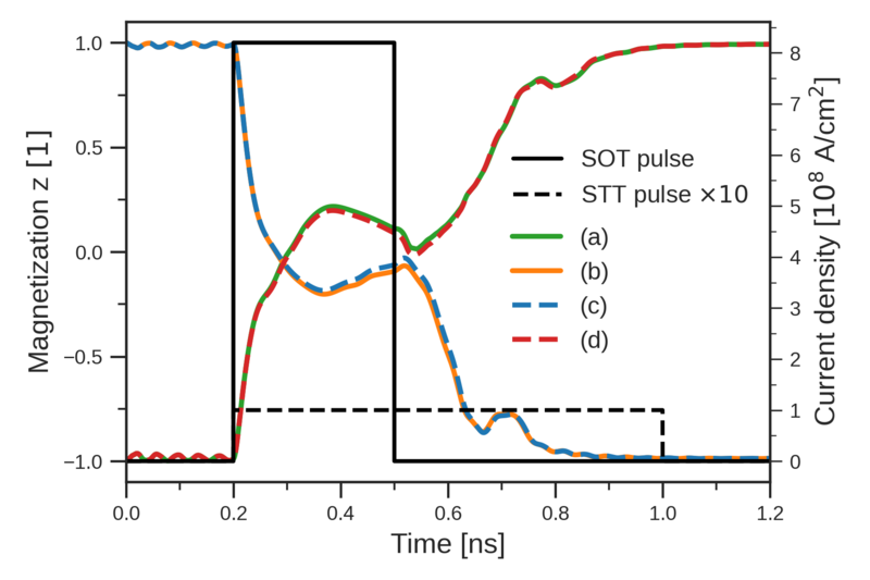
Figure 8.8: The \(z\)-component of the volume averaged magnetization and the applied current as a function of time. The four possible switching modes are shown.
(a): \(-z\) to \(+z\) switching, with SOT pulse along \(-x\) and STT pulse along \(-z\).
(b): \(+z\) to \(-z\) switching, with SOT pulse along \(+x\) and STT pulse along \(+z\).
(c): \(+z\) to \(-z\) switching, with SOT pulse along \(-x\) and STT pulse along \(+z\).
(d): \(-z\) to \(+z\) switching, with SOT pulse along \(+x\) and STT pulse along \(-z\).
At the top contact a voltage of \({\mathbin {\textpm }} 4.0\,\si {V}\) is applied, at the left SOT contact a voltage of \({\mathbin {\textpm }} 0.20\,\si {V}\) is applied, while the right SOT contact is kept grounded.
This results in a current density through the MTJ of \(j^\mathrm {P}_\mathrm {STT} \approx -1.0\times 10^{7} \, \si {A/cm^2}\) along the \(\mp z\) direction for a parallel (P) state, \(j^\mathrm {AP}_\mathrm {STT}
\approx 0.3\times 10^{7} \, \si {A/cm^2}\) for an antiparallel (AP) state, and a current density of \(j_\mathrm {SOT} \approx 8 \times 10^{8} \, \si {A/cm^2}\) through the SOT layer along the \(\mp x\) direction.
The switching of the FL is driven by a combined SOT and STT current pulses applied for \(0.3\,\si {ns}\) and \(0.8\,\si {ns}\), respectively, the resulting time evolution of the \(z\)-component of the magnetization is shown
in Fig. 8.8. Four different switching modes are possible depending on the initial magnetization direction of the FL, the direction of the SOT current pulse, and the direction
of the STT current pulse. Switching from \(-z\) to \(+z\) (P\(\to \)AP) can be achieved with a SOT current pulse along \({\mathbin {\textpm }} x\) if the STT current pulse is along \(-z\), while switching from \(+z\) to
\(-z\) (AP\(\to \)P) can be achieved with a SOT current pulse along \({\mathbin {\textpm }} x\) if the STT current pulse is along \(+z\). In contrast to the previous devices, the different switching modes give slightly
different switching dynamics. Most notably, the AP\(\to \)P switching is faster than the P\(\to \)AP switching, which is to be expected, as this is also observed with pure STT switching.
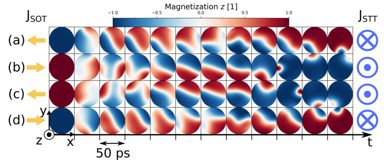
Figure 8.9: The spatial distribution of the \(z\)-component of the magnetization in the center of the FL at different time steps during the switching process. Each snapshot is taken at 50 ps intervals from the moment the
pulse is applied. The four possible switching modes (a-d) are shown, where the yellow and blue arrows indicate the direction of the SOT pulse and the STT pulse, respectively.
The spatial distribution of the magnetization is shown in Fig. 8.9 at different time steps during the switching process for all four switching modes. The switching dynamics
exhibit a similar domain wall nucleation behavior to that observed for switching with an external field, except that a second domain wall forms, which combines with the first. The nucleation of the second domain wall occurs on the
edge opposite to the SOT current flow, suggesting a complex interplay between the DMI, SOTs, and STTs. The second domain wall is thus aligned or anti-aligned with the first for P\(\to \)AP and AP\(\to \)P switching,
respectively. The combined unswitched domain then rotates around the edge of the FL while shrinking until the switching is complete. The switching process is notably faster for AP\(\to \)P switching modes compared to P\(\to
\)AP switching modes, which is expected, as pure STT switching exhibits similar characteristics.
STT-assisted SOT switching is an effective FFS scheme; nonetheless, as a hybrid of the two, it inherits the advantages and disadvantages of both. Compared to conventional SOT switching, the scalability is improved due to the
elimination of the external field; however, the need for a strong current through the MTJ increases the energy consumption and introduces endurance concerns due to the stress on the TB, while a weaker current takes away the
sub-ns switching speed advantage of SOT switching. Compared to conventional STT switching, the faster speed and zero incubation time come at the cost of a larger footprint.