Another promising FFS scheme was demonstrated by Garello et al. in 2019 [149], achieving field-free operation without compromising writing speed, energy efficiency, or endurance. In this approach, a thick Co layer with an
in-plane magnetization is incorporated into the cell to generate an in-plane stray field in the FL, which acts analogously to the external magnetic field. The approach was presented as highly integration-friendly, utilizing devices
fabricated on a 300 mm wafer with CMOS-compatible processes. Moreover, the stray field-generating Co layer was embedded in the hardmask used to form the SOT track during the fabrication process, allowing for BEOL process
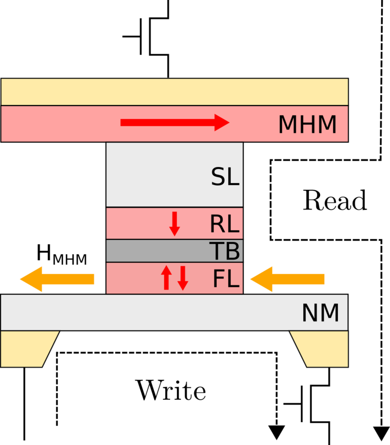
compatibility, which is essential for a smooth integration with existing manufacturing processes. Figure 8.10a shows a schematic of the device where the magnetic hardmask
(MHM) is placed above the MTJ with a SL in between. The magnitude of the stray field depends on the thickness of the MHM and the distance between the MHM and the FL, which can be adjusted by changing the thickness of
the SL between them. The direction of the stray field is antiparallel to the MHM magnetization, which is permanently fixed during fabrication.
(a) Device
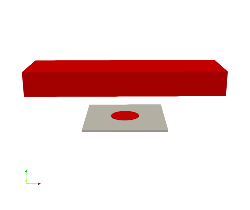
(b) Mesh
Figure 8.10: Schematic of a MHM-SOT-MRAM device with PMA (a), and the corresponding mesh used for the simulations (b). Red arrows indicate the magnetization direction of the MHM, FL, and RL, while the yellow
arrows indicate the direction of the MHM stray field. The dashed lines indicate the path of the read and write currents.
The mesh used for the simulations is shown in Fig. 8.10b. The geometry is the same as the one used with the external field, neglecting the TB and RL, except for the addition of
a MHM above the FL. The bottom MHM interface is located \(80\) nm above the upper FL interface. To ensure that the stray field is sufficiently strong a MHM thickness of \(50\) nm is used. Moreover, to keep the stray field
uniform in the FL, the MHM is made \(120\) nm wide, and \(390\) nm long. The MHM magnetization is fixed along the \(+x\) direction, and the magnetization saturation is set to \(M_s = 1.44\) MA/m, which is typical for
hexagonal close-packed Co [15]. Parameters corresponding to W and CoFeB are used for the SOT layer and the FL, respectively. The SOT layer is set to a thickness of \(3.5\,\si {nm}\) to maximize the SOTs in the \(\beta
\)-W phase. The resulting mesh consists of approximately \(35000\) elements.
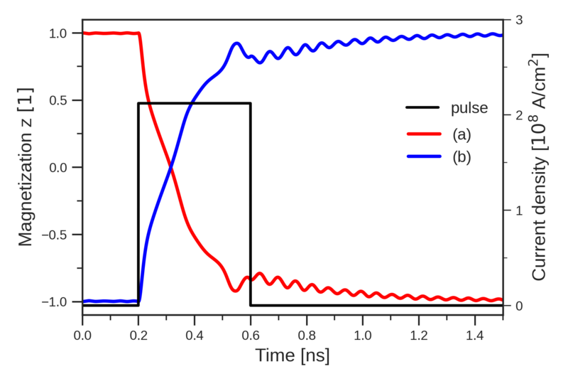
Figure 8.11: The \(z\)-component of the volume averaged magnetization and the applied current density as a function of time. The red curve shows the switching from \(+z\) to \(-z\) with a current along \(+x\) (a), while
the blue curve shows the switching from \(-z\) to \(+z\) with a current along \(-x\) (b).
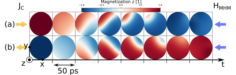
Figure 8.12: The spatial distribution of the \(z\)-component of the magnetization in the center of the FL at different time steps during the switching process. Each snapshot is taken at 50 ps intervals from the moment the
pulse is applied. The four possible switching modes (a-d) are shown, where the yellow and blue arrows indicate the direction of the SOT pulse and MHM stray field, respectively.
A voltage bias of \(0.50\,\si {V}\) is applied across the W layer, resulting in a current density of \(j_\mathrm {SOT} \approx 2 \times 10^{8} \, \mathrm {A/cm^2}\) along the \(x\) direction. The magnetization switching
is driven by a \(0.4\,\si {ns}\) pulse and the time evolution is shown in Figs. 8.11 and 8.12. Switching from \(+z\) to \(-z\) is
achieved with a current pulse along \(+x\), while switching from \(-z\) to \(+z\) is achieved with a current pulse along \(-x\), due to the negative spin Hall angle of W opposite current directions are required for the switching
compared to the results for an external field presented earlier. As expected, the switching dynamics are similar to those with an external field, where a domain wall nucleates at the edge and propagates diagonally to the current
direction across the FL to the opposite edge. The precession observed previously is much less pronounced here, thus the magnetization dynamics are more in line with the experimental observations reported by Baumgartner et
al. [145]. This is mainly due to the switching having progressed further by the time the current pulse is turned off. However, micromagnetic simulations have shown that a strong positive ratio of FL to DL torque, as seen in
W/CoFeB, speeds up the switching process, whereas a negative ratio, as observed in Pt/CoFeB, slows it down [145].
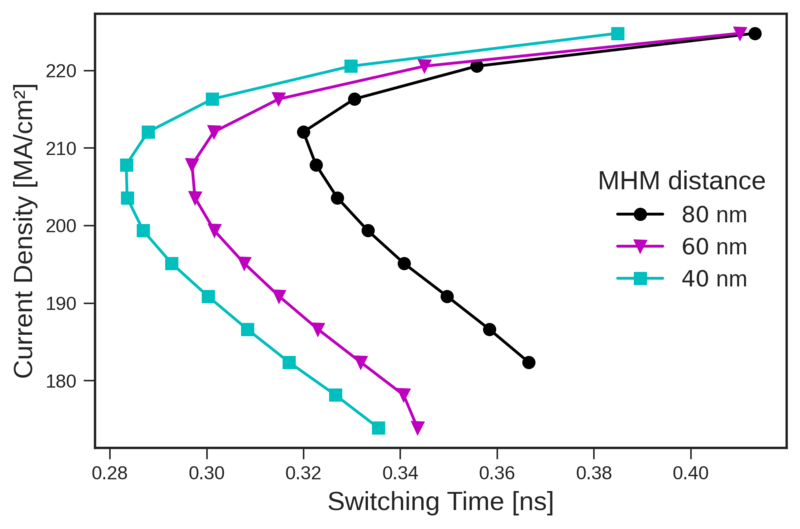
Figure 8.13: Applied current density versus switching time for FFS with MHM. The simulations were performed on the mesh shown in Fig. 8.10b for a range of current
densities and different positions of the MHM relative to the FL. The MHM, FL, and NM layers were modeled as Co, CoFeB, and W, respectively.
As the strength of the stray field is determined by the material and the volume of the MHM, along with the distance between the MHM and FL, the window of possible switching current densities is limited, as switching is only
possible when the stray field and SOTs are comparable in strength, as the combination of both is required. Figure 8.13 shows the switching current density required as a
function of the achieved switching time for different distances between the MHM and FL. The switching time improves with increasing switching current density, reaching a minimum around \(0.32-0.34\) ns, thereafter the
switching time quickly increases with increased \(j_\mathrm {W}\). Improvements in the switching current density and switching time can be obtained by reducing the SL thickness from \(80\) nm to \(40\) nm. However, the
improvements are only minor and show signs of saturation. Further improvements of this design require a larger MHM volume or a material with a higher saturation magnetization.