6.2 One-Dimensional Charge and Spin
Drift-Diffusion
Experimental systems for probing SOTs often consist of homogeneous multilayer stacks with widths and lengths that are significantly larger than the thicknesses of the layers. In such cases, the system can be effectively treated as
1D, and material parameters such as the spin diffusion length and spin Hall angle can be extracted by fitting 1D analytical solutions of the spin drift-diffusion equations to the experimental data. In this section, the general solution
of the charge and spin drift-diffusion equations in 1D is presented, along with a generalized method for solving the resulting boundary value problem for a given set of layers and BCs. This method is used to study the BCs presented
in the previous chapter, extract relevant parameters from experimental data, and test the numerical implementation of the full 3D drift-diffusion equations.
6.2.1 General Solution of the Charge and Spin
Drift-Diffusion Equations in One Dimension
Assuming a constant in-plane electric field along \(x\), and that the spin accumulation and spin current density are homogeneous in the \(xy\)-plane, the charge and spin drift-diffusion equations can be reduced to one dimension.
The charge and spin current densities along the \(z\) direction can then be expressed as
respectively. Here \(I\) is the \(3\times 3\) identity matrix, \([\bm {m}]_\times \) is the cross product matrix defined as \(\left (\left [\bm {x}\right ]_\times \right )_{ij} = \varepsilon _{ikj} x_k \), such
that \([\bm {x}]_\times \bm {y} = \bm {x}\times \bm {y} \), for the vectors \(\bm {x}\) and \(\bm {y}\).
For a NM layer (\(\bm {m} = \bm {0}\)), with its lower and upper interface at \(z_i\) and \(z_{i+1}\), respectively, the general solution of Eqs. (6.7) and (6.8) is
\(\seteqnumber{1}{6.11}{0}\)
\begin{align}
V_c(z) & = az + b, \qquad \text {and} \\ \bm {V_s}(z) & = \bm {A}e^{\frac {z-z_{i+1}}{\lambda _{sf}}} + \bm {B}e^{\frac {-(z-z_i)}{\lambda _{sf}}},
\end{align}
respectively, where the unknown coefficients \(a\), \(b\), \(\bm {A}\), and \(\bm {B}\), are determined by the BCs. The expressions for the current densities are obtained by inserting Eqs. (6.11) into Eqs. (6.6), which gives
For a FM layer with a uniform magnetization direction, the general solution reads
\(\seteqnumber{1}{6.13}{0}\)
\begin{align}
V_c(z) & = az + b +\beta _D\bm {V^F_s}(z)\cdot \bm {m}, \\ \bm {V_s}(z) & = \sum _i \bm {v_i} \left [A_i e^{\frac {z-z_{i+1}}{\lambda _{i}}} + B_i e^{\frac {-(z-z_i)}{\lambda
_{i}}}\right ],
\end{align}
where \(\bm {v_i}\) are the eigenvectors of the matrix \(\tilde {M}^{-1} \tilde {N}\), and \(\lambda _i\) are the corresponding eigenvalues. The coefficients \(a\), \(b\), \(A_i\), and \(B_i\) need to be determined by the
BCs. Using \(\partial _z V_c(z) = a +\beta _D\partial _z\bm {V^F_s}(z)\cdot \bm {m}\), the current densities in the FM layer can be expressed as
Figure 6.3: Sketch of the 1D multilayer system and the labeling scheme for the layers and interfaces.
Considering a multilayer system with \(N\) layers, there are two external boundaries at \(z_0\) and \(z_{N} \), and \(N-1\) internal boundaries at \(z_i\) for \(i = 1,\dots ,N-1\). A sketch of the 1D system is shown in
Fig. 6.3. At external boundaries, it can be assumed that there is zero flux of currents:
\(\seteqnumber{1}{6.15}{0}\)
\begin{align}
j^1_{\alpha z}(z_0) & = 0, \\ j^{N}_{\alpha z}(z_{N}) & = 0.
\end{align}
The subscript denotes the spin polarization and charge component \(\alpha \in [x,y,z,c]\), while the superscript denotes the layer. For the spin components \(j^i_{\alpha z} = (e/\mu _B)J^i_{\alpha z}\). Alternatively,
if the external boundaries are contacts, the electrical potential is fixed with Dirichlet BCs, and the spin current is determined by Robin BCs:
For the internal boundary \(i\) with adjacent layers \(i\) and \(i+1\), assuming the spin accumulation and current are continuous across the internal boundaries, the following BCs are considered:
Inserting the expressions for the general solution for the currents and potentials into the BCs and collecting the terms proportional to the unknown coefficients on the left-hand side and the terms independent of the coefficients on
the right-hand side allows for a linear system of equations to be assembled for each interface. For the external boundaries, the following two systems of equations are obtained:
where \(\bm {x_{i}}\) is the vector of unknown coefficients for the potentials and spin accumulations in layer \(i\), \(C_{i,j}\) is the matrix for interface \(i\) and layer \(j\). For the internal boundaries, the following linear
system of equations is obtained:
which can be solved using standard linear algebra methods, such as LU factorization [83].
6.2.4 Implementation and Validation of the One-
Dimensional Charge and Spin Drift-Diffusion Solver
The 1D charge and spin drift-diffusion (1D-CSDD) solver is implemented in Python using functions from the NumPy library for scientific computing [84]. The implementation is object-oriented, consisting of classes for the layers
and interfaces that contain the respective parameters and equations. The solver class assembles the system of equations for a given multilayer system and solves it using the LU factorization solver provided by NumPy. The
implementation allows for easy modification of the system parameters, such as layer thicknesses, material properties, and BCs, making it suitable for testing different scenarios.
To validate the implementation, a typical NM/FM bilayer system is considered. At the external boundaries, there is zero flux of currents, and the NM/FM interface is described by the BCs from the MCT. The analytical solution of
this system is derived and presented in Appendix B, which will be used to validate the numerical results. The interface is placed at \(z = 0\) and
each layer has a thickness of \(20\) nm.
.
Parameter
NM
FM
Unit
\(D_e\)
0.01
0.01
m\(^2\)/s
\(\sigma \)
\(5\)
\(5\)
MSm\(^{-1}\)
\(\alpha _\mathrm {SH}\)
\(0.059\)
\(1\)
\(\beta _\sigma ,\beta _D\)
\(0.46\)
\(1\)
\(\lambda _\mathrm {sf}\)
\(2.57\)
\(69.3\)
nm
\(\lambda _{J}\)
\(2.0\)
nm
\(\lambda _{\phi }\)
\(0.1\)
nm
(a) Bulk parameters
.
Parameter
Value
Unit
\(\operatorname {Re}[G_{\uparrow \downarrow }]\)
\(5.95 \times 10^{14}\)
Sm\(^{-2}\)
\(\operatorname {Im}[G_{\uparrow \downarrow }]\)
\(0.86 \times 10^{14}\)
Sm\(^{-2}\)
\(G_{\uparrow \uparrow }\)
\(6.66 \times 10^{14}\)
Sm\(^{-2}\)
\(G_{\downarrow \downarrow }\)
\(3.96 \times 10^{14}\)
Sm\(^{-2}\)
(b) Interface parameters
Table 6.1: The bulk and interface parameters used for the NM/FM bilayer. The interface conductances are calculated from the analytical expressions presented in Appendix
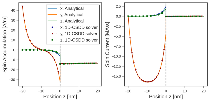
Figure 6.4: 1D analytical and 1D-CSDD solver solutions for the spin accumulation (a) and spin current density (b) distributions in a NM (20 nm)/FM (20 nm) bilayer system. The results were obtained using the parameters
listed in Table 6.1.
Figure 6.4 shows the analytical and numerical results for the spin accumulation and spin current obtained using the parameters listed in Table 6.1, an in-plane electric field of \(10^6\) V/m, and a magnetization direction along \((1,1,1)\). The results show a good agreement between the analytical and numerical
solutions. The normalized mean absolute error (NMAE) between the analytical and numerical solutions is given by
where \(v_i\) and \(v_{h,i}\) is the analytical and numerical solution evaluated at position \(z_i\), respectively. The 1D system was discretized into \(n=4000\) points using a step size of \(h = 0.01\,\mathrm {nm}\). Using
Eq. 6.23 for each spin component and taking the norm of the spin accumulation and spin current, a total NMAE of \(0.17\%\) and \(0.80\%\) is obtained for the spin
accumulation and spin current density, respectively, verifying the validity of the numerical implementation.